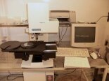
Used NANOMETRICS NanoSpec 6100 #9021461 for sale
URL successfully copied!
Tap to zoom


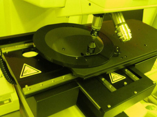

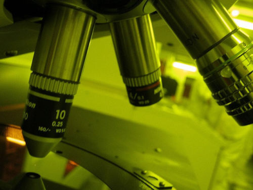

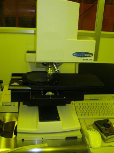

ID: 9021461
Wafer Size: Up to 8"
Vintage: 2001-2002
Film thickness analyzer, up to 8"
2001-2002 vintage.
NANOMETRICS NanoSpec 6100 is a high-performance mask and wafer inspection equipment desgined to provide high accuracy and repeatability for mask and wafer inspection and defect control. The system leverages the latest in imaging and measurement technologies to ensure that only the highest quality designs and wafers can be produced. NanoSpec 6100 inspects mask and wafer defects with sub-micron resolution and accuracy, utilizing advanced pattern recognition algorithms and measuremnt techniques to identify and mark out any outliers in the design. The unit uses RapidScan laser imaging for mask alignment and verification, enabling high-accuracy inspection of entire mask patterns and wafers, even in larger design space. The machine also features a high-resolution camera allowing for image capture of the acquired material for post-analysis. It is capable of providing simultaneous focus, shift, and magnification measurements, and has a built-in programmable illumination tool. A wide range of customizable parameters are available, including optical correction to reduce user calibration costs. NANOMETRICS NanoSpec 6100 includes a range of automated test routining and defect measurement capabilities, allowing streamlined analysis and optimization of design models, as well as advanced defect masking. It offers its users flexible programming capabilities and robust automation of test patterns and defect measurement analysis. For high-throughput applications, NanoSpec 6100 is also available with a multi-chamber, 4-field 10-wafer automated station. This station is capable of simultaneously testing and analyzing 10 wafers, with up to 4 different field images per wafer. This saves significant time when testing complex arrays and elements. NANOMETRICS NanoSpec 6100 is a versatile and powerful tool for analyzing and optimizing wafer and mask designs. With its high count resolution, repeatable results, and automated testing routines, users can be confident that they are getting the highest quality and accuracy in their designs and wafers.
There are no reviews yet
