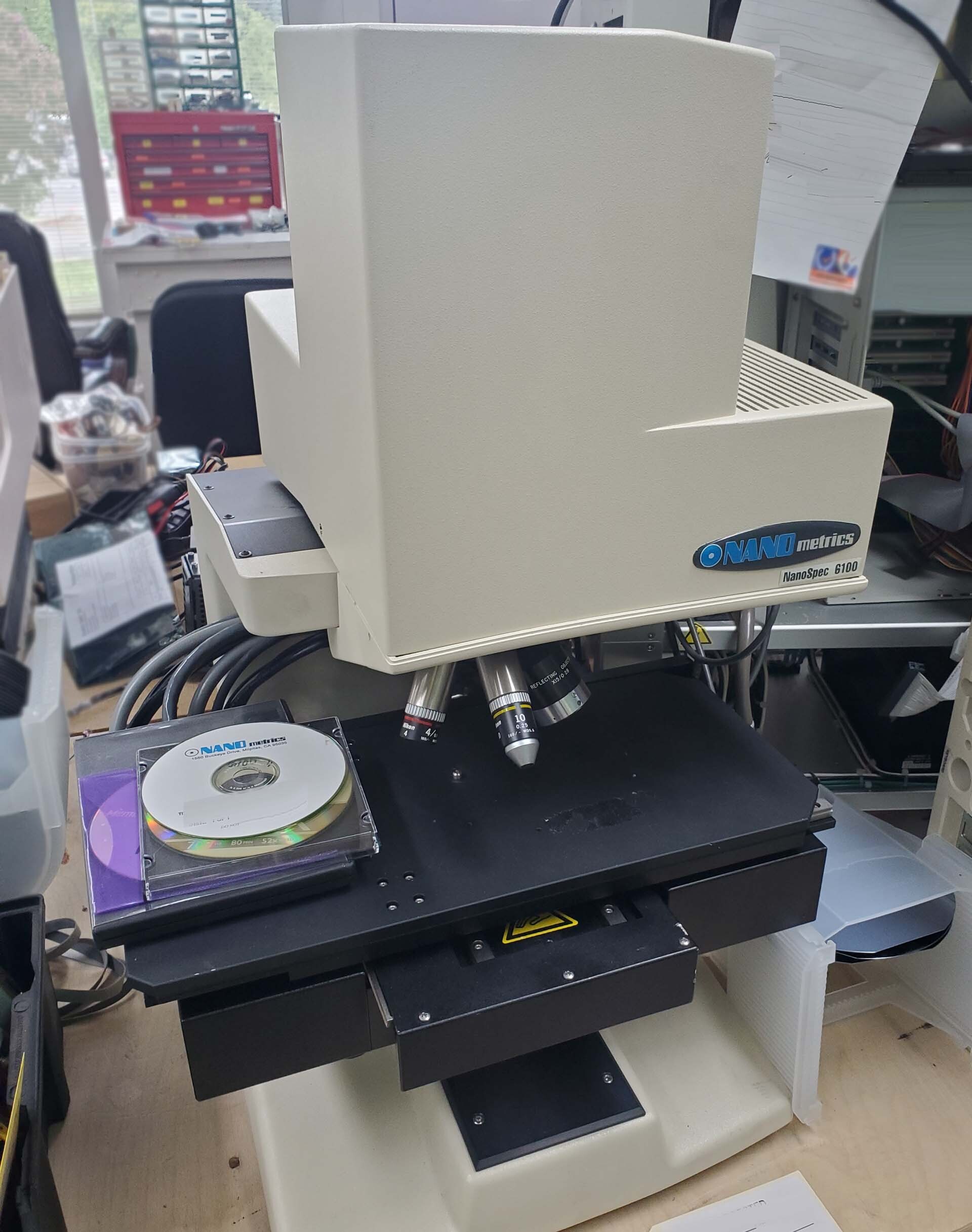
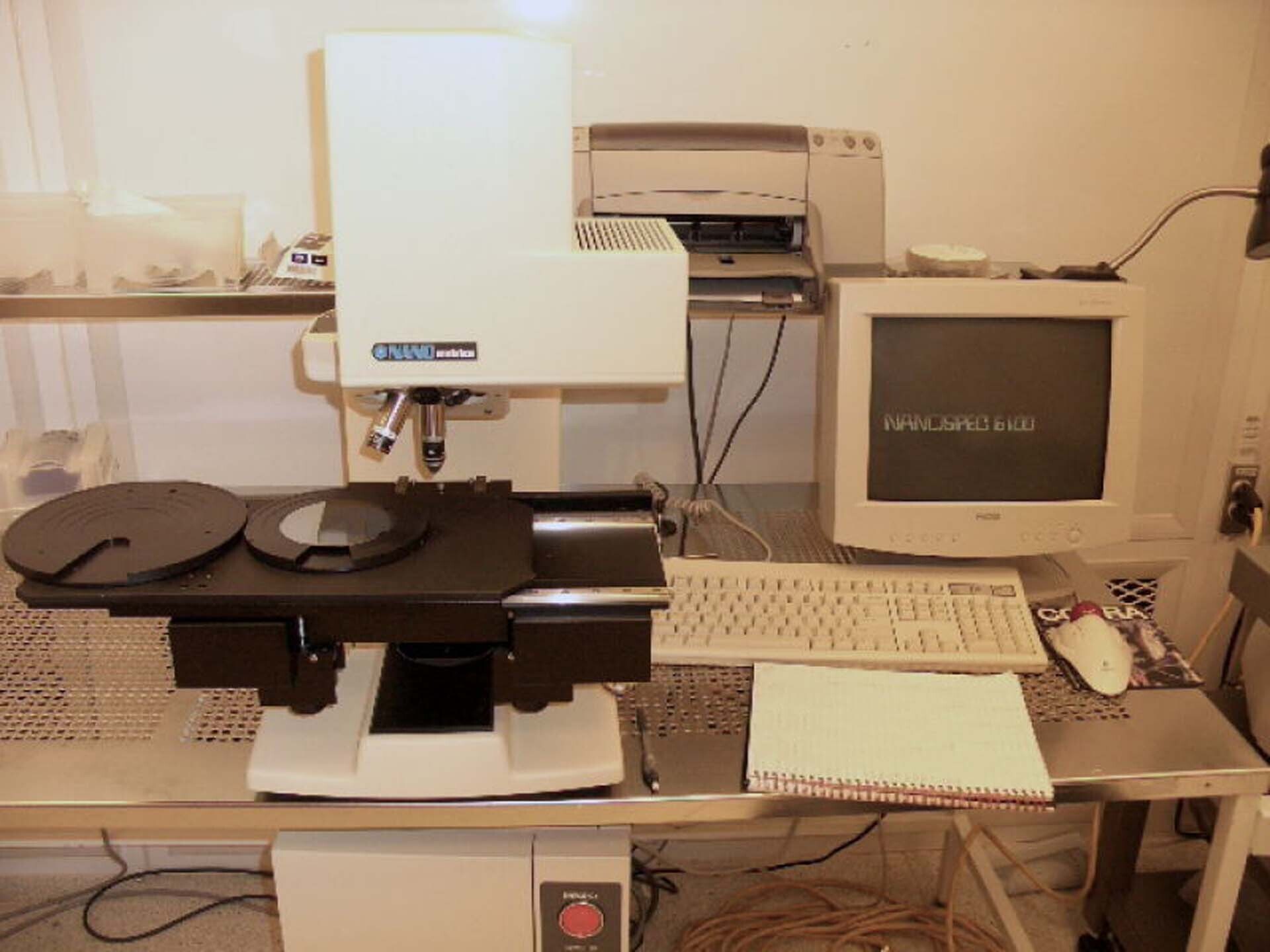
Used NANOMETRICS NanoSpec 6100 #9355328 for sale
URL successfully copied!
Tap to zoom


ID: 9355328
Wafer Size: 3"-8"
Film thickness measurement systems, 3"-8"
Films: Up to 3-layers
Wavelength range: 400 to 800 nm
Film thickness range:
Visible: 250Å to 20 μm
UV and visible: 40Å to 20 μm (Dependent on film type)
Reproducibility: < 1Å UV / 2Å (Visible)
Measurement time: 0.5-3 Sec/site
Data management: 2D and 3D Mapping / Diameter scan
Communication type: SECS II
Data export: ASCII
Optics: 4x, 10x, 15x (UV), 40x
Spot sizes: 50 / 20 / 18 (UV) / 5.5 μm
PC System with high capacity drives
LCD Screen
Tabletop components:
Optics stand
Monitor and keyboard
Mouse
Trackball and joystick
Control electronics (WxDxH):
14" x 24" x 28"
35.56 x 60.96 x 71.12 cm
Power supply: 117 ±5% VAC, 50/60 Hz, 5 A.
NANOMETRICS NanoSpec 6100 is a leading edge mask and wafer inspection equipment that helps semiconductor manufacturers ensure the highest levels of production quality. The system incorporates a high power (100-watt) laser diode, a large field-of-view camera, and a suite of advanced optics and image processing algorithms. NanoSpec 6100 enables automated inspection of defect features as small as 3.5nm on both mask and wafer surfaces and is capable of rapid detection of lithographic hotspots, particles, scratches, and other critical defects. NANOMETRICS NanoSpec 6100 utilizes a 100-watt laser diode to project light in a large, rectangular field-of-view that is scanned across the surface of the substrate. The unit's optics are designed to minimize distortion and light scatter, allowing it to detect sub-wavelength defects and surface features with high fidelity. The resulting images are analyzed in real-time by image segmentation algorithms, allowing defects to be identified and flagged for further inspection. NanoSpec 6100 uses two advanced imaging modes to provide maximum flexibility and robustness. In RGB imaging mode, the machine utilizes a high-resolution color sensor to detect defects in both mask and wafer substrates. In contrast, in single-wavelength imaging mode, a single laser wavelength is used to perform threshold-based detections of both large and small particles, scratches, pits, and other defects. NANOMETRICS NanoSpec 6100 also offers a high degree of automation and flexibility. A large touchscreen display allows operators to easily start and stop inspections, change settings, and analyze results. Additionally, the tool's high speed scanning capability and automated defect recognition provide unparalleled throughput and performance. Overall, NanoSpec 6100 is a superb mask and wafer inspection asset that provides industry-leading performance. With high resolution imaging and powerful automated algorithms, the model is capable of rapid and reliable detection of lithographic defects and critical surface features. It is a powerful tool for achieving the highest levels of quality and production yield in modern semiconductor manufacturing.
There are no reviews yet

