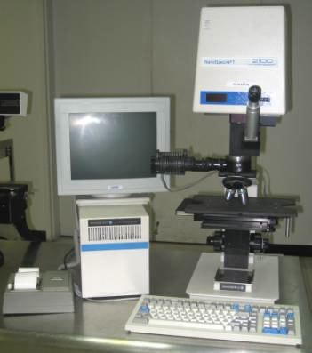
Used NANOMETRICS NanoSpec AFT 2100 #96637 for sale
URL successfully copied!
Tap to zoom


ID: 96637
Wafer Size: 4"-8"
Automatic film thickness system, 4"-8"
Model 7000-0410 Rev. P2
Model 7200-1750 Rev. A Computer
Model 7200-0410 Measurement head
100 to 500,000 Angstroms range of thickness
NIKON M Plan 10X & 40X Objective lenses
Manual sliding stage for 5” & 6” Wafers
Databank 2 storage system with 14 standard programs
Video display monitor
SECS-2 Communication interface
20 Column thermal printer.
NANOMETRICS NanoSpec AFT 2100 is a comprehensive mask and wafer inspection equipment. Using advanced scanning and imaging technology, the system is capable of detecting minute defects in masks and wafers used in semiconductor fabrication processes. The unit also offers automated defect classification, providing a systematic process for inspectors to quickly and accurately identify defects in large yields of devices. The AFT 2100 utilizes visible light to detect and analyze microscopic defects in both masks and wafers. It has a highly sensitive optical head and a brighter incident light source which enables accurate representation of complex topologies and enables high-speed inspection. The machine also incorporates spectral analysis, enabling it to detect minute differences in spectral reflectance in various defects, such as voids, contaminants, and cracks. The AFT 2100 is equipped with state-of-the-art image processing algorithms and user-friendly image analysis tools that enable rapid identification of defects. It can automatically classify individual defects and determine their criticality. The tool has a built-in integrity calculator which identifies systemic defects. It also offers automated yield summary and analysis, making it easier to analyze large yields of wafers and masks. The AFT 2100 also includes a highly efficient defect elimination asset. This model assists inspectors with defect reduction, allowing them to quickly and accurately identify and eradicate defects, increasing the overall quality of wafers and masks manufactured. Furthermore, the equipment is capable of rapidly averaging images of tested wafers, reducing the total time for inspection and analysis. The AFT 2100 is a reliable and versatile mask and wafer inspection system; offering accuracy, speed and ease of use. It provides inspectors with an efficient, effective and cost-effective solution for identifying and eliminating defects in masks and wafers. Its combination of deep imaging resolution, spectral analysis, defect identification, classification and integrity calculator makes it an invaluable tool for semiconductor manufacturers.
There are no reviews yet