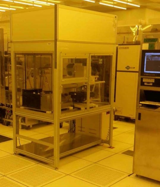
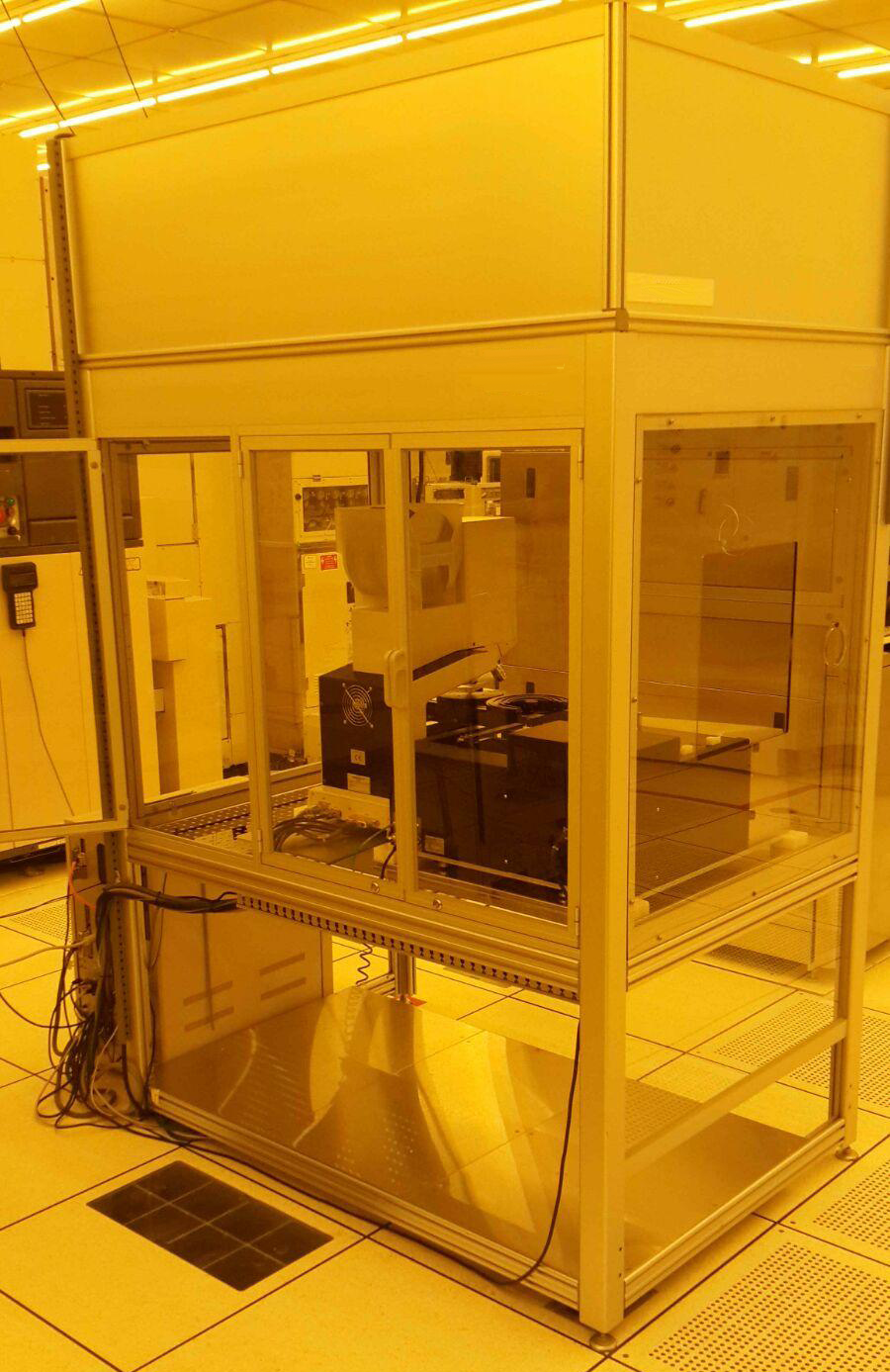
Used NANOMETRICS NanoSpec AFT 6100 #9276360 for sale
URL successfully copied!
Tap to zoom


ID: 9276360
Film thickness measurement system
Handler: OLYMPUS AL110 Series Auto loader
Up to (3) layers
Reproducibility: <1Å UV, 2Å (Visible)
Measurement time: 0.5 to 3 sec/site
Data management: 2D and 3D Mapping, diameter scan
Communication kit: SECS II
Data export: ASCII
Wave length range:
400 to 800 nm
210 to 800 nm
Film thickness range:
250Å to 20µm (Visible)
40Å to 20µm (UV and visible)
Components:
Optics stand
Monitor
Key board
Track ball
Joy stick
Hardware configuration:
Wafer size: 75 mm to 200 mm
Optics: 4x, 10x, 15x (UV), 40x
Spot size: 50, 20, 18 (UV), 5.5 µm
PC Computer with high capacity drives
Power supply: 117 ±5% VAC, 50/60 Hz, 5 A.
NANOMETRICS NanoSpec AFT 6100 is a precision mask and wafer inspection equipment designed to ensure optimal product yield by detecting manufacturing defects as small as a single nanometer. It can detect virtually any patterning issue, including misalignments, lack of process coverage, etch process defects, wafer cracks, misalignment of features, and other anomalies. NanoSpec AFT 6100 works by taking ultra high-resolution images of mask and wafer patterns along with defect maps. This is then used to analyze features at the nanometer level, providing detailed insights on defect patterns, location, and size. It also assists in measuring the photomask feature accuracy, placement and alignment accuracy, and pattern integrity. The AFT 6100 has a high-resolution camera with up to 50 megapixel resolution and a patented digital image acquisition system, which enables the detection of very small defects. The software architecture of the unit includes a powerful image capturing and defect detection engine, flexible data analysis and comparison tools, and extensive reporting capabilities. The machine has a zooming capability up to 332X, allowing a high level of magnifications to be used to view localized defects. It's equipped with transparent chuckers which are used to enforce the flatness and placement accuracy of a wafer or mask. NANOMETRICS NanoSpec AFT 6100 also has an automated optical alignment tool that can quickly align a photomask with the wafer template, helping reduce the inspection time. NanoSpec AFT 6100 offers a highly flexible and reliable inspection asset with high accuracy and precision. Its intuitive graphical user interface also allows users to quickly find and understand defect information. The model can be used for production, qualification and process development work at many different levels, from the single die to equipment level. The AFT 6100 is easy to use and offers a variety of options for customization to meet specific needs. It is an essential tool for any wafer manufacturing process that requires extreme precision and detail in patterning and inspection capabilities.
There are no reviews yet


