Used NANOMETRICS NanoSpec II #293766064 for sale
URL successfully copied!


Tap to zoom
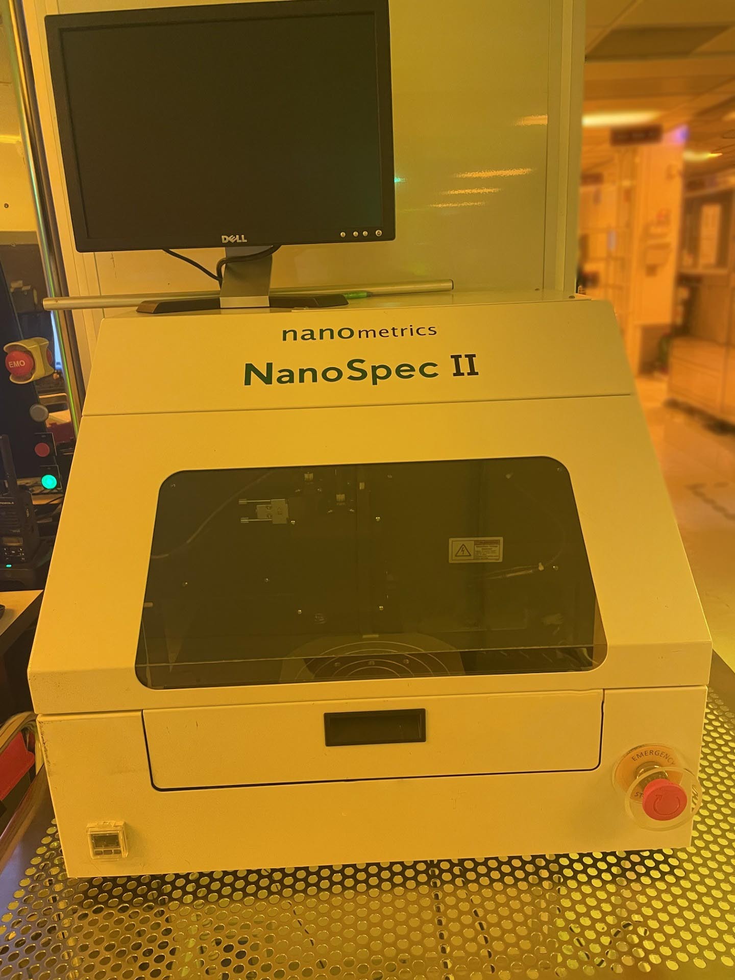

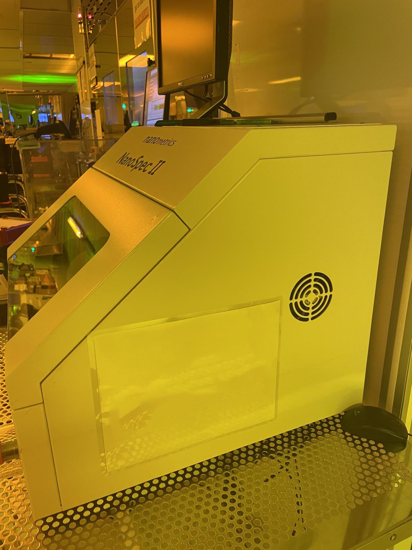
NANOMETRICS NanoSpec II is a mask and wafer inspection equipment developed by NANOMETRICS to accurately detect defects as small as 0.1µm. NanoSpec II is designed to deliver the highest quality imaging available in the market with easy integration into complex semiconductor workflows. This new system boasts high resolution imaging with up to 128x magnification, allowing for optimal defect analysis. Its path splitting functionality utilizes multiple sensors to inspect a single die, reducing inspection time and increasing overall throughput. Additionally, its unique ASMI (Adaptive Sub-Pixel Motion Interpolation) technology compensates for sample deformation, ensuring consistently accurate defect identification. Moreover, NANOMETRICS NanoSpec II offers a wide field of view and full domain measurements with true overlay for critical overlay defect analysis. The unit acquires all available light data for maximum image mimicking, including darkfield, brightfield and polarization. NanoSpec II is also equipped with a full suite of automated defect classification algorithms to efficiently sort through potential defect sites. Fewer false positive defect sites are reported, reducing the need to manually review glyph images for inspection. Additionally, color enhancement technology renders defect images into their true colors to increase classification accuracy. This patent-pending machine, integrated into NANOMETRICS calibration plat-form, offers easy installation and excellent image uniformity across varying field sizes to reduce test cost. Its easy to use software platform simplifies tool configuration, offering automated tool and sample inspections, image capture and defect review, improving the efficiency of the entire mask and wafer inspection process. NANOMETRICS NanoSpec II is an ideal solution for manufacturers requiring improved wafer defect sensitivity, high productivity, and designed for those who need an intuitive, easy to use inspection asset. Its high precision imaging capabilities are the perfect choice for manufacturers looking to improve workflow speed and accuracy.
There are no reviews yet