Used NANOMETRICS NanoSpec II #293773923 for sale
URL successfully copied!

Tap to zoom
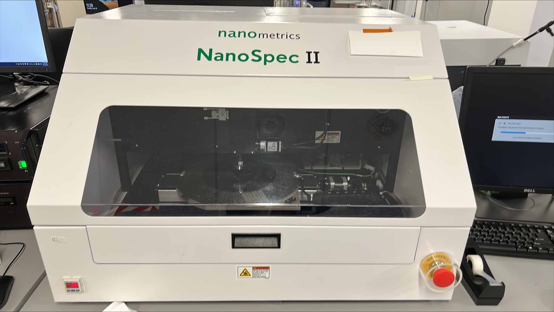

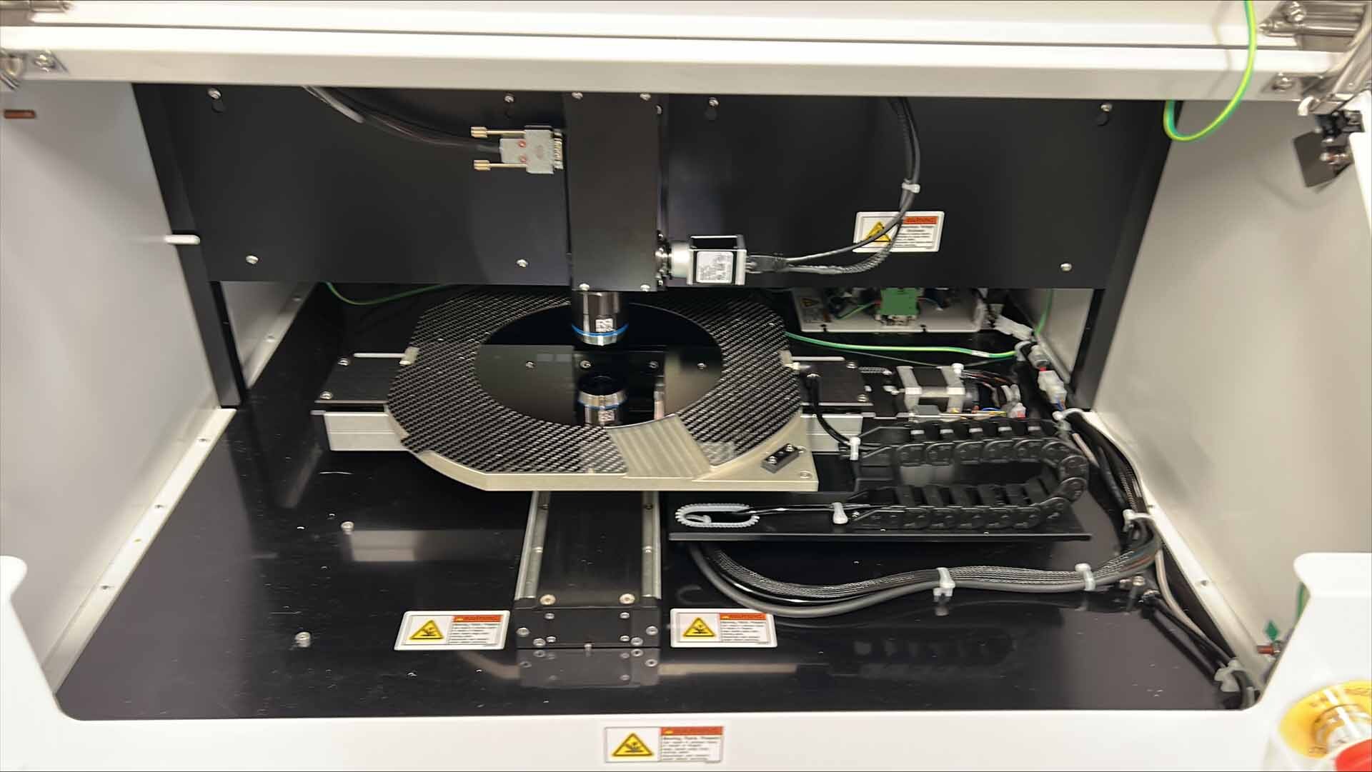
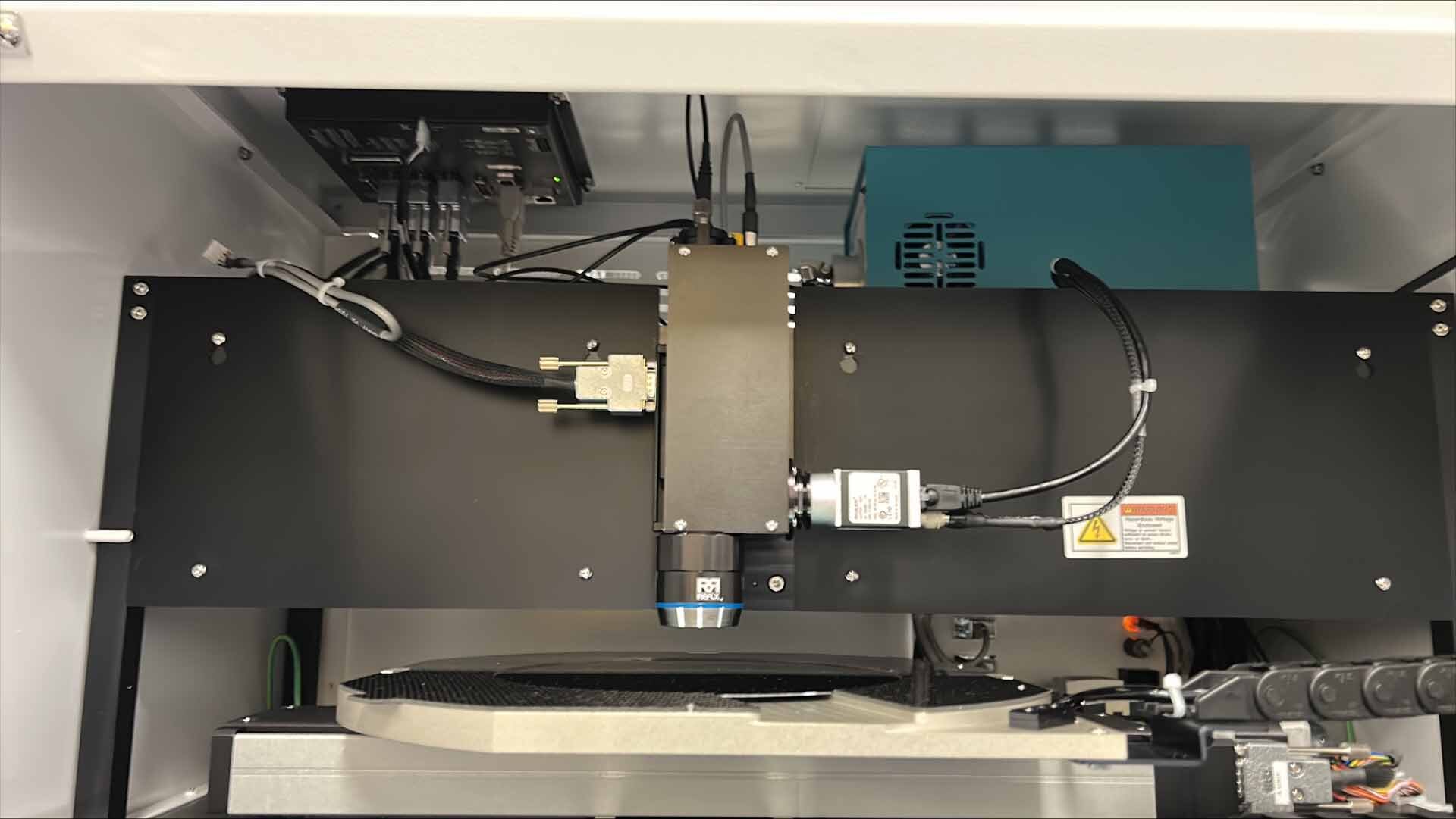
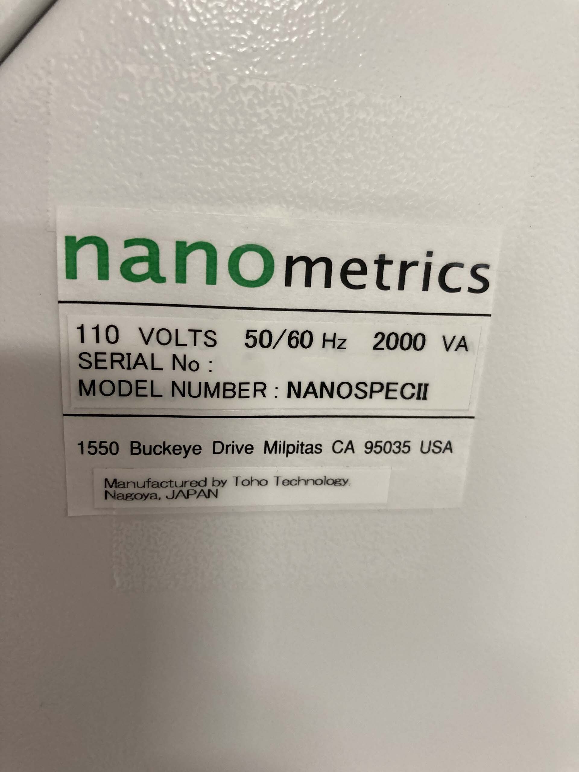
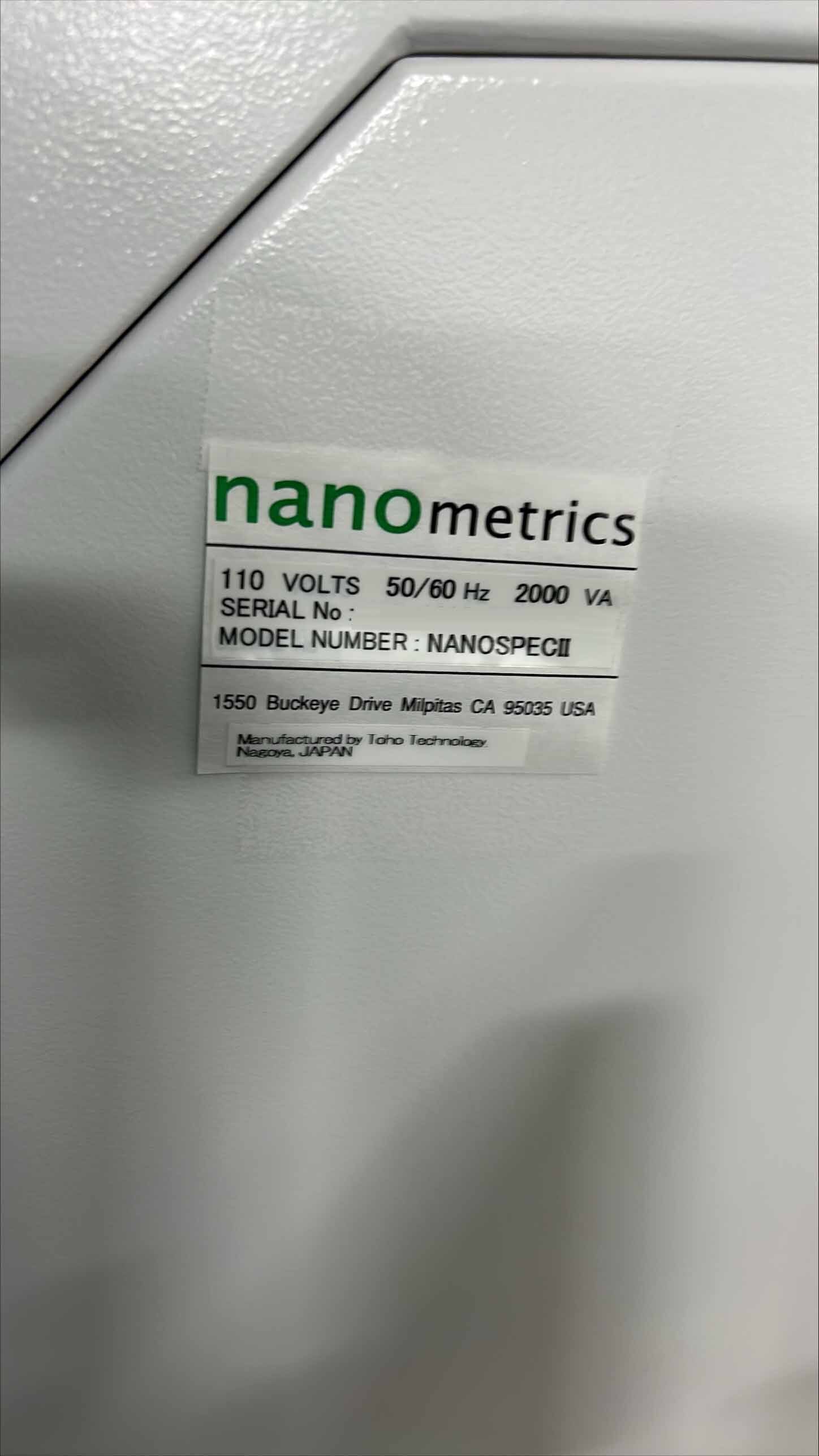
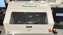
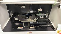
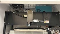
NANOMETRICS NanoSpec II is an advanced mask and wafer inspection equipment designed to meet the rigorous demands of semiconductor manufacturing. This cutting-edge tool leverages state-of-the-art technology to provide high-resolution inspection capabilities that enable semiconductor manufacturers to achieve superior quality control and process optimization. Key Features: 1. High-resolution Imaging: NanoSpec II is equipped with high-resolution imaging technology that enables the detection of nanometer-sized defects on masks and wafers. This unparalleled level of sensitivity allows manufacturers to identify and address even the smallest defects, ensuring the production of high-quality semiconductor devices. 2. Multiple Inspection Modes: NANOMETRICS NanoSpec II offers multiple inspection modes to accommodate different types of defects and inspection requirements. Whether it's surface defects, particle contamination, or pattern deviations, this system is capable of detecting and analyzing various types of defects with precision and accuracy. 3. Automated Inspection Process: One of the standout features of NanoSpec II is its automated inspection process. The unit is equipped with advanced algorithms and machine learning capabilities that enable automated defect detection and classification. This automation streamlines the inspection process, reduces human error, and increases overall efficiency in semiconductor manufacturing. 4. Real-time Analysis: NANOMETRICS NanoSpec II provides real-time analysis of inspection results, allowing manufacturers to quickly identify and address any defects during the production process. This feature enables proactive defect mitigation, minimizing production downtime and ensuring consistent product quality. 5. User-friendly Interface: The machine is designed with a user-friendly interface that simplifies operation and reduces the learning curve for operators. The intuitive interface provides easy access to inspection settings, result visualization, and data analysis tools, empowering users to make informed decisions and optimize their semiconductor manufacturing processes. 6. Compatibility: NanoSpec II is compatible with a wide range of masks and wafers used in semiconductor manufacturing, making it a versatile tool for various applications. Whether working with advanced photomasks or cutting-edge silicon wafers, this tool delivers reliable and consistent inspection results across different material types and substrates. 7. Scalability and Future-proofing: As semiconductor technology continues to evolve, NANOMETRICS NanoSpec II is designed to be scalable and future-proof. The asset can be upgraded with the latest software updates and hardware enhancements to adapt to changing industry requirements and keep pace with technological advancements. In summary, NanoSpec II is a state-of-the-art mask and wafer inspection model that offers advanced imaging capabilities, automated inspection processes, real-time analysis, user-friendly interface, compatibility with various substrates, and scalability for future-proofing. By leveraging the power of this cutting-edge tool, semiconductor manufacturers can achieve superior quality control, increased productivity, and optimized manufacturing processes in the dynamic semiconductor industry.
There are no reviews yet