Used NIKON NSR 2205 i14E2 #293725478 for sale
URL successfully copied!
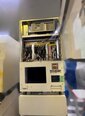

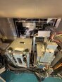
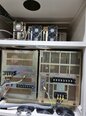
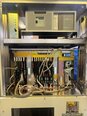


Tap to zoom

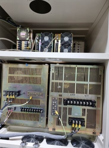
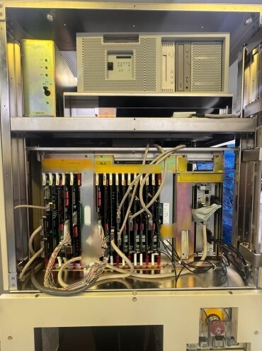
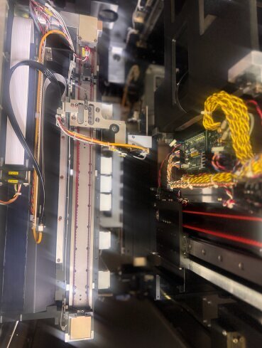
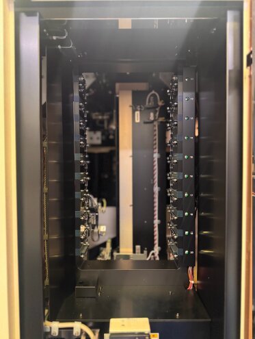
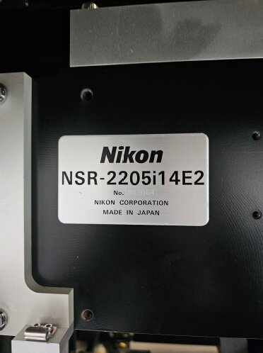
ID: 293725478
Wafer Size: 8"
Vintage: 2001
Stepper, 8"
Lamp Power: 847.096㎽/㎠
Lamp Uniformity: 4.450%
Repeatability (3sigma n-1) 0.036um
Step-X (3σ): 0.019 ㎛
Step-Y (3σ): 0.017 ㎛
Magnification: 1/5 Reduction
Light Source: i‑Line (365 nm)
Resolution: 0.35 µm
Lens NA: 0.50–0.63 Variable
Exposure Field Size: 22 mm (up to 17.9H × 25.2V)
Control: Bellows Unit
Lens Adjustment: Micrometer / PIEZO / Washer
Lamp: 2.5 kW Hg Lamp
PC System Type: DMCC
No UPS System
Reticle Size: 5-6"
Alignment Sensor LSA
Alignment Sensor FIA
No Alignment Sensor LIA
Alignment Sensor TTLFC2
Measure Software
Illumination System: SHRINC4 Type
Interferometer Type: 5517C
Interferometer Wafer Stage
Interferometer Reticle Stage
Focus System: Multi Focus
Leveling System: Table
Wafer Loader Type: Type 3
Wafer Orientation / Notch: OF or Notch
Wafer Loader Wafer Size: 8"
(2) Cassettes
Wafer In‑Line: Left In‑Line (DNS)
Wafer Pre‑Alignment Type: NC PRE2
No Wafer Edge Exposure
Reticle Loader Type: Normal
Reticle Barcode Reader
Particle Checker
Signal Tower
ASAHI SENDAI N4A‑C Chamber
Electrical Power Spec: 208 V / 60 Hz / 3‑Phase
2001 vintage.
NIKON NSR 2205 i14E2 is an advanced wafer stepper designed for high-volume semiconductor manufacturing, particularly in the production of integrated circuits (ICs) and other microelectronic devices. This state-of-the-art equipment combines precision alignment, ultra-high resolution imaging, and advanced patterning capabilities to enable the fabrication of intricate nanostructures on silicon wafers with exceptional accuracy and repeatability. At the heart of NIKON NSR-2205I14E2 is a sophisticated projection optical system that utilizes deep ultraviolet (DUV) light sources to achieve sub-micron resolution. The unit features a high-numerical aperture (NA) lens with multiple lens elements to focus the DUV light onto the wafer surface, enabling the printing of extremely small features with sub-100 nm critical dimensions. The advanced optics also incorporate adaptive illumination and aberration correction techniques to optimize image quality and pattern fidelity across the entire wafer. One of the key strengths of NSR-2205 I14E2 is its exceptional overlay accuracy, which is critical for aligning multiple layers of patterns on the wafer during the lithography process. The machine utilizes an advanced alignment stage with multiple degrees of freedom, coupled with sophisticated image processing algorithms, to achieve sub-nanometer alignment precision between different mask layers. This enables the fabrication of complex, multi-layered structures with tight registration requirements, such as those found in advanced memory and logic devices. In addition to its superior alignment capabilities, NSR 2205I 14E2 offers a range of advanced patterning modes to accommodate various lithography requirements. The tool supports both contact and proximity lithography modes, allowing for the patterning of different feature sizes and aspect ratios on the wafer. It also features a variable numerical aperture (VNA) function, which enables the user to adjust the resolution and depth of focus of the projection optics to suit different patterning needs. To enhance productivity and reduce cycle times, NSR-2205I14E2 is equipped with automated wafer handling and alignment systems. The asset features robotic wafer loaders and unloaders, as well as advanced wafer alignment sensors and algorithms, to ensure rapid and accurate wafer positioning during the lithography process. This high level of automation not only improves throughput but also minimizes operator intervention, reducing the risk of human errors and increasing overall process efficiency. Overall, NSR 2205 i14E2 represents the cutting edge of wafer stepper technology, offering semiconductor manufacturers a powerful tool for achieving sub-micron lithography requirements with exceptional precision and reliability. With its advanced optics, precise alignment capabilities, and automated functionality, this model is ideally suited for producing the next generation of microelectronic devices with ever-increasing levels of complexity and performance.
There are no reviews yet