Used NIKON Optistation VII #9225598 for sale
URL successfully copied!
Tap to zoom
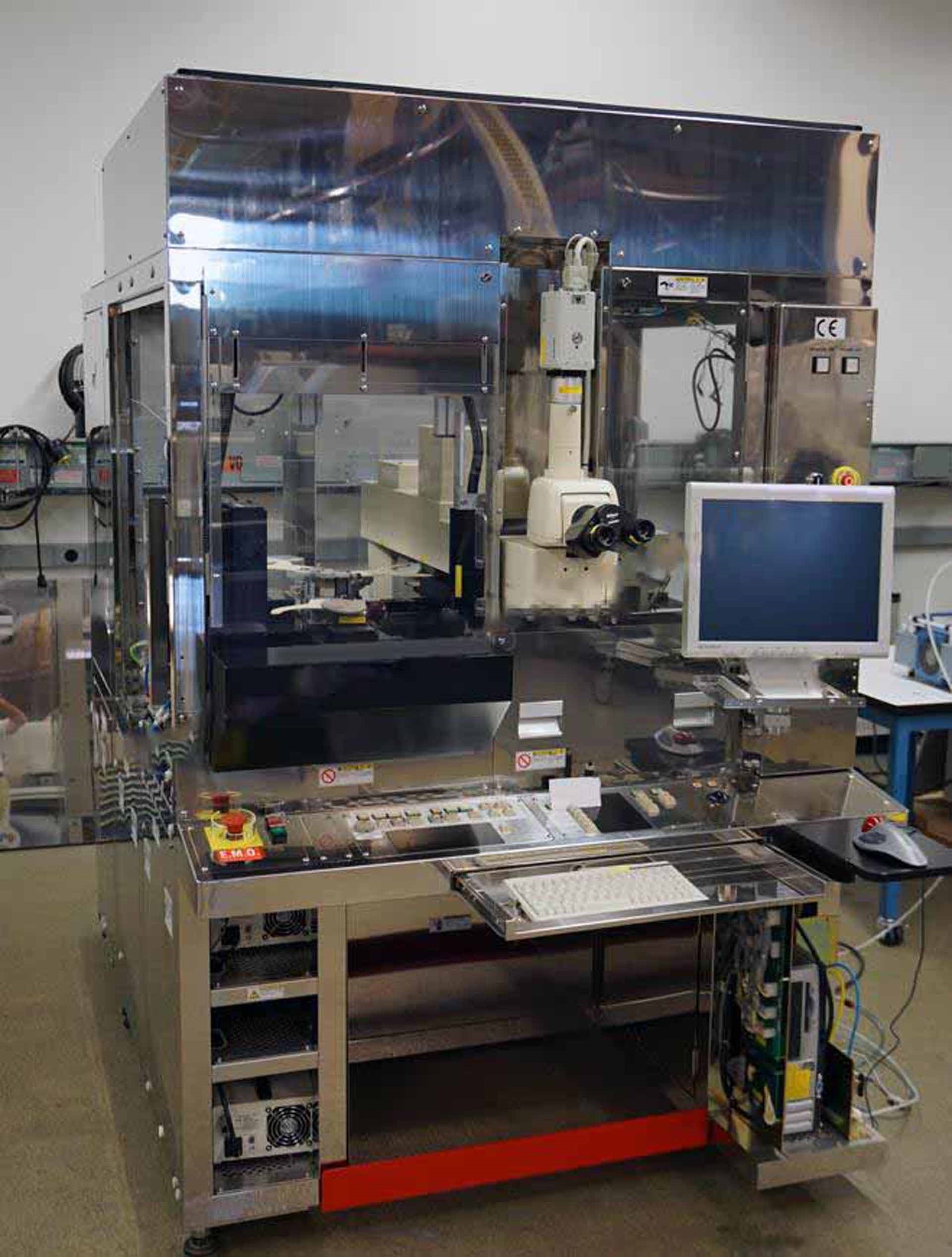

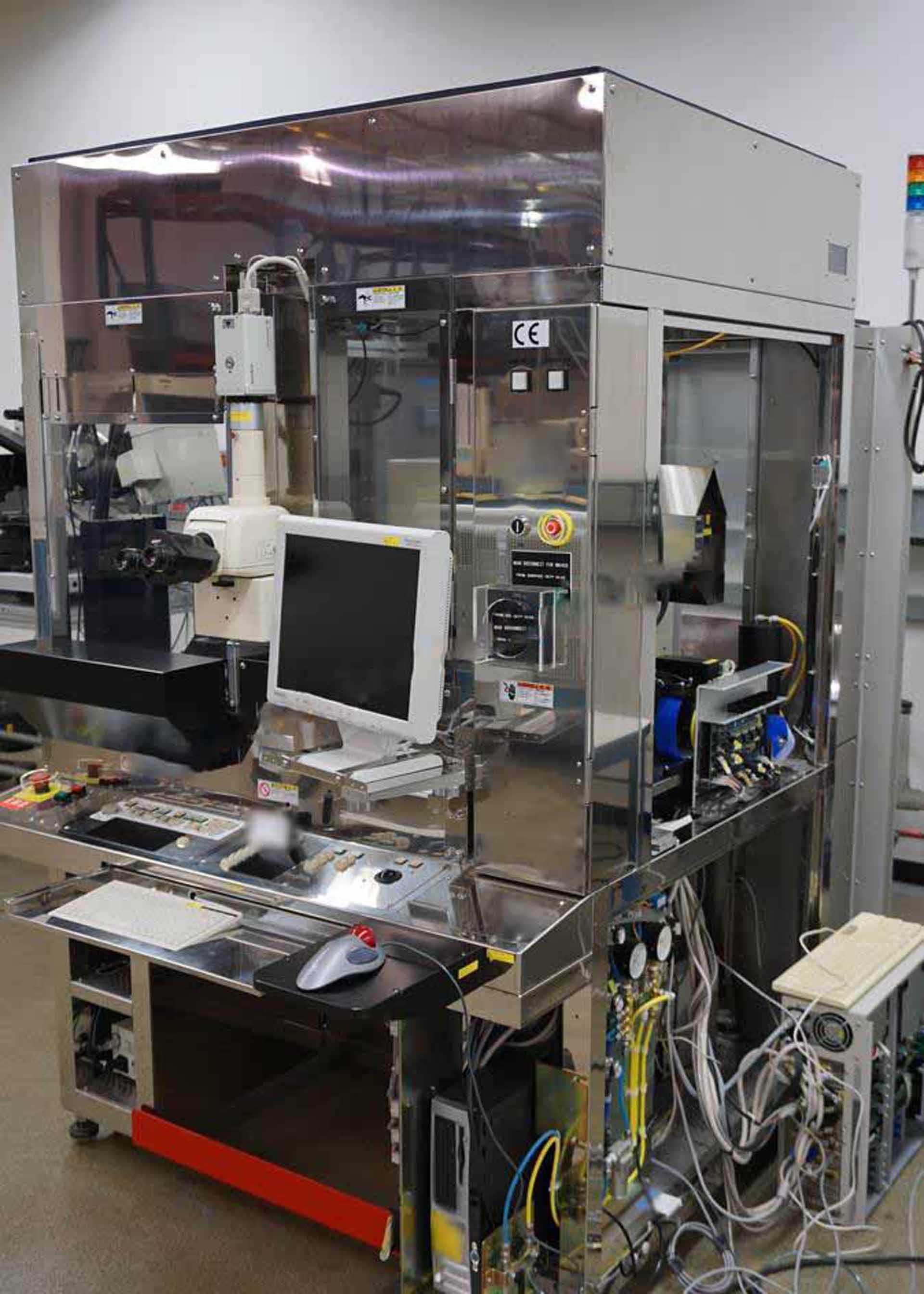

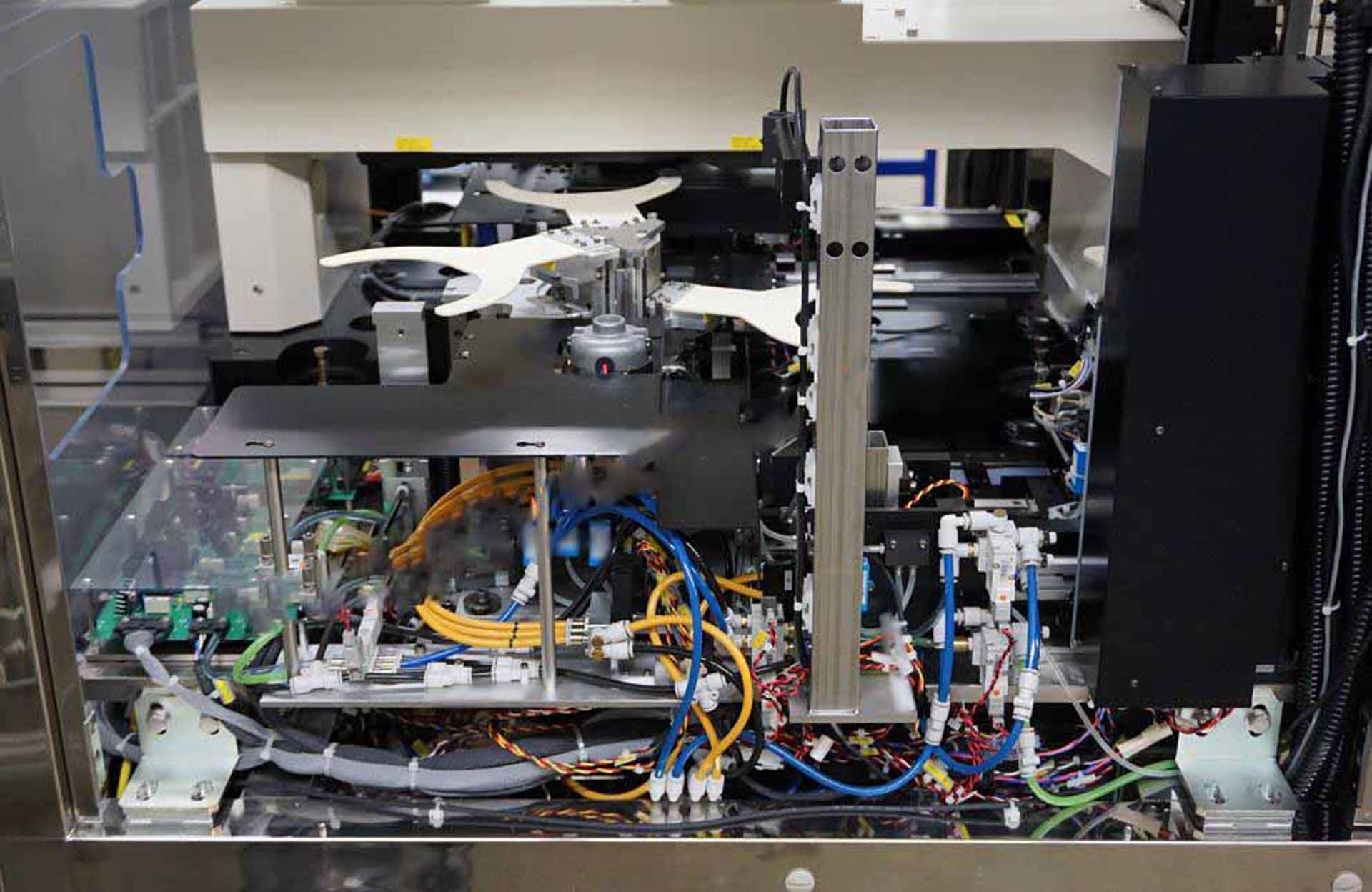


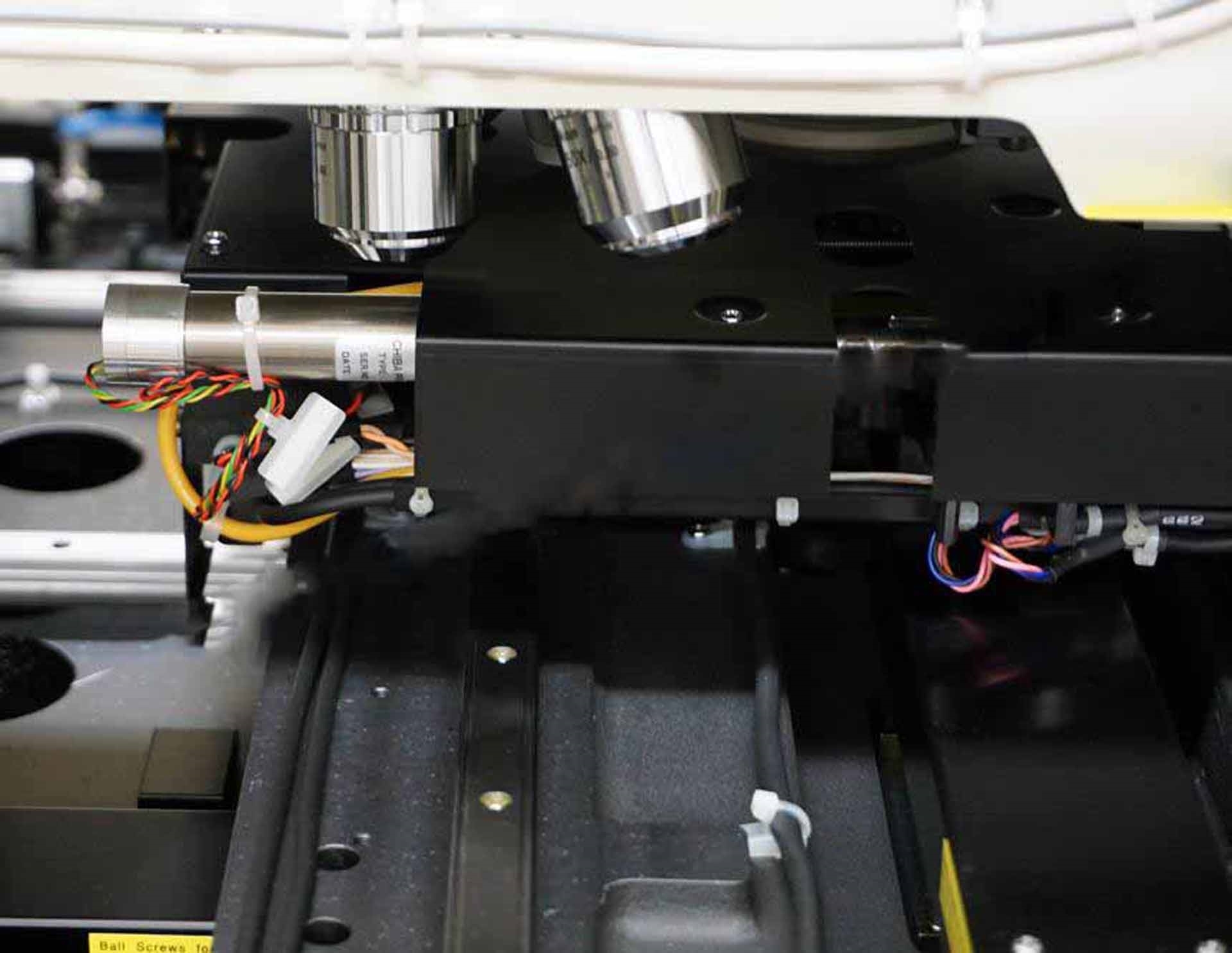

ID: 9225598
Wafer Size: 12"
Automated inspection station, 12"
With FOUP loaders
(2) FOUP Front end load ports:
ASYST ISO Port FL300
With mapper and RFID
Integrated ULPA filtration system
Air suspension vibration isolation table
Standard microscope unit with automated control
10x Eyepieces
Objective lens:
2.5x N.A 0.075 W.D 8.8 mm
10x N.A 0.300 W.D 6.50 mm
20x N.A 0.460 W.D 3.10 mm
50x N.A 0.900 W.D 0.42 mm
150x N.A 0.900 W.D 0.29 mm
Halogen lamp house: 12 V, 100 Watt
Robot and robot controller
Ceramic robot arm
Ceramic rotation arm
Macro unit (A): Wafer chuck
Macro movable uni
Slider assembly
Macro unit (B): Arched holder
Rotation unit assembly
Micro stage unit:
XY Stage / Chuck
X, Y, Z Drive units
Dart controller for image archiving and defect review
LCD Display
Keyboard & trackball
Image capture board
SONY Camera: DXC-9XX/MD.
NIKON Optistation VII is an advanced mask & wafer inspection equipment that features an integrated, high-resolution wafer-level camera, ultra-high resolution optics, advanced illumination techniques, and sophisticated software. Optistation VII allows for the fast, accurate and non-destructive inspection of masks and wafers used in the manufacture of semiconductor integrated circuits. With its advanced features, NIKON Optistation VII offers a comprehensive system for inspecting masks and wafers and finding defects, anomalies and pattern imperfections. Optistation VII is designed for optical inspection of both metal and photomasks, with a specially designed microscope that allows for a maximum field view of 10x and a maximum resolution of 20.4μm, to ensure an accurate inspection. A reflectance spectrophotometer is integrated for colorimetric measurements and NIKON Optistation VII is capable of detecting the slightest irregularities in mask reflections, specular highlights, and other forms of material imperfections. Optistation VII also has a high-resolution wafer-level camera, allowing for the examination of structures at the precision level of 16nm. The camera features a CMOS image sensor with a field of view of 3.8mm wide and a resolution of 1.5um, with a maximum data rate of 56Gbps. The camera can be adjusted to various focus distances, allowing for the best resolution and illumination of the material being studied. The inspection unit offers a variety of advanced illumination techniques, including polarized, scattered, and oblique lighting that can be used to study and analyze the minutest features possible. NIKON Optistation VII is equipped with powerful image processing software that can detect and measure a wide array of defects, such as pinholes, smudges, lines and pattern imperfections. Defects are identified in real time and the software can create a detailed report with quantitative defect analysis. Optistation VII provides a powerful and flexible mask & wafer inspection machine for a wide range of industries. With its high-resolution optics, advanced illumination methods, and software for detecting and analyzing defects, NIKON Optistation VII allows for the efficient inspection of masks and wafers with top-tier accuracy and precision.
There are no reviews yet


