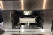
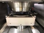
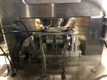
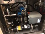
Used OBDUCAT Eitre 6 #9260763 for sale
URL successfully copied!
Tap to zoom





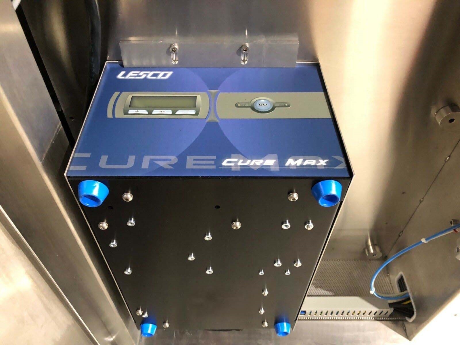

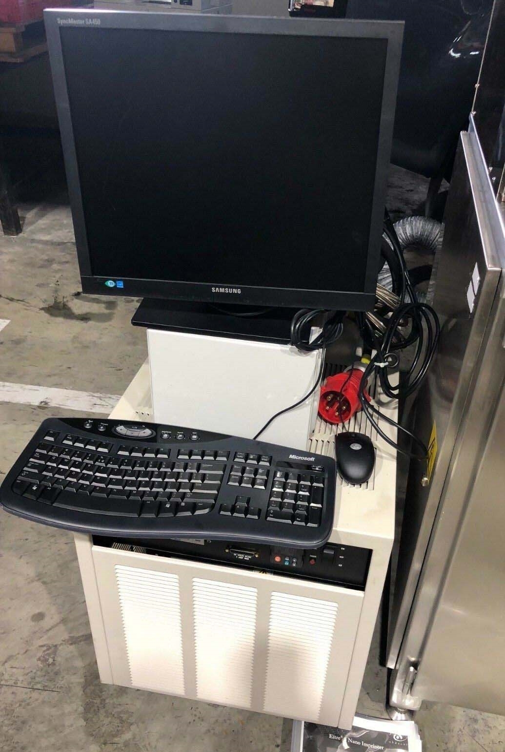


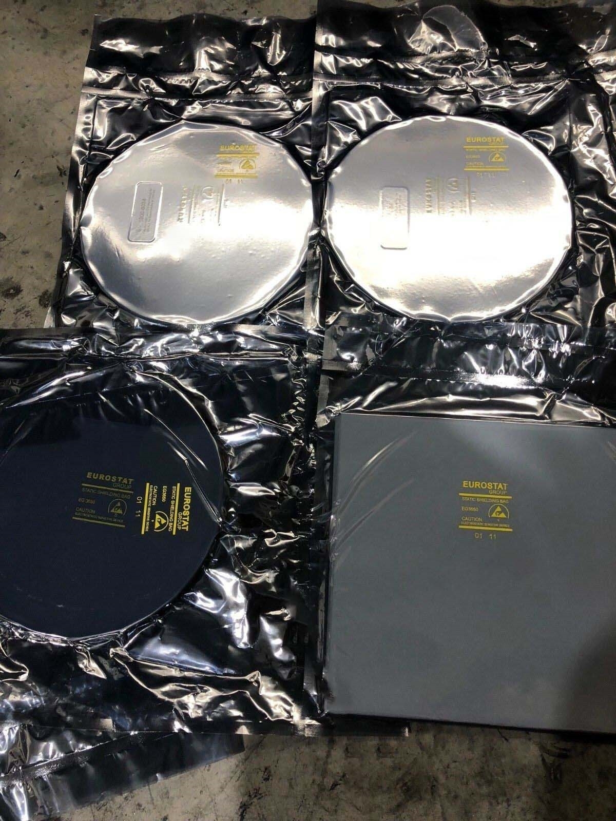

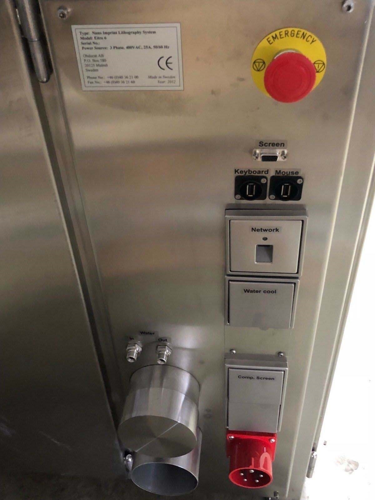

ID: 9260763
Wafer Size: 6"
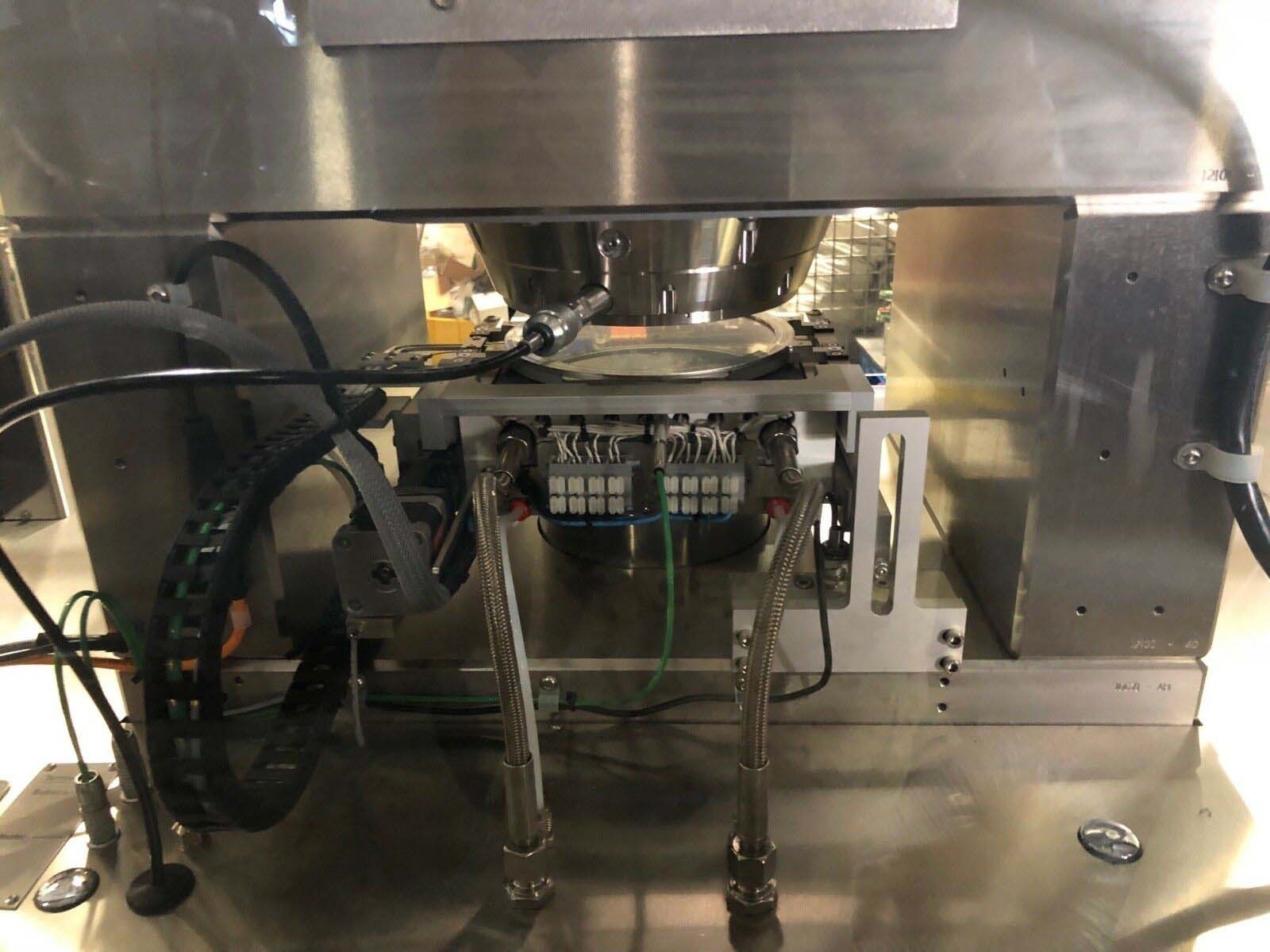
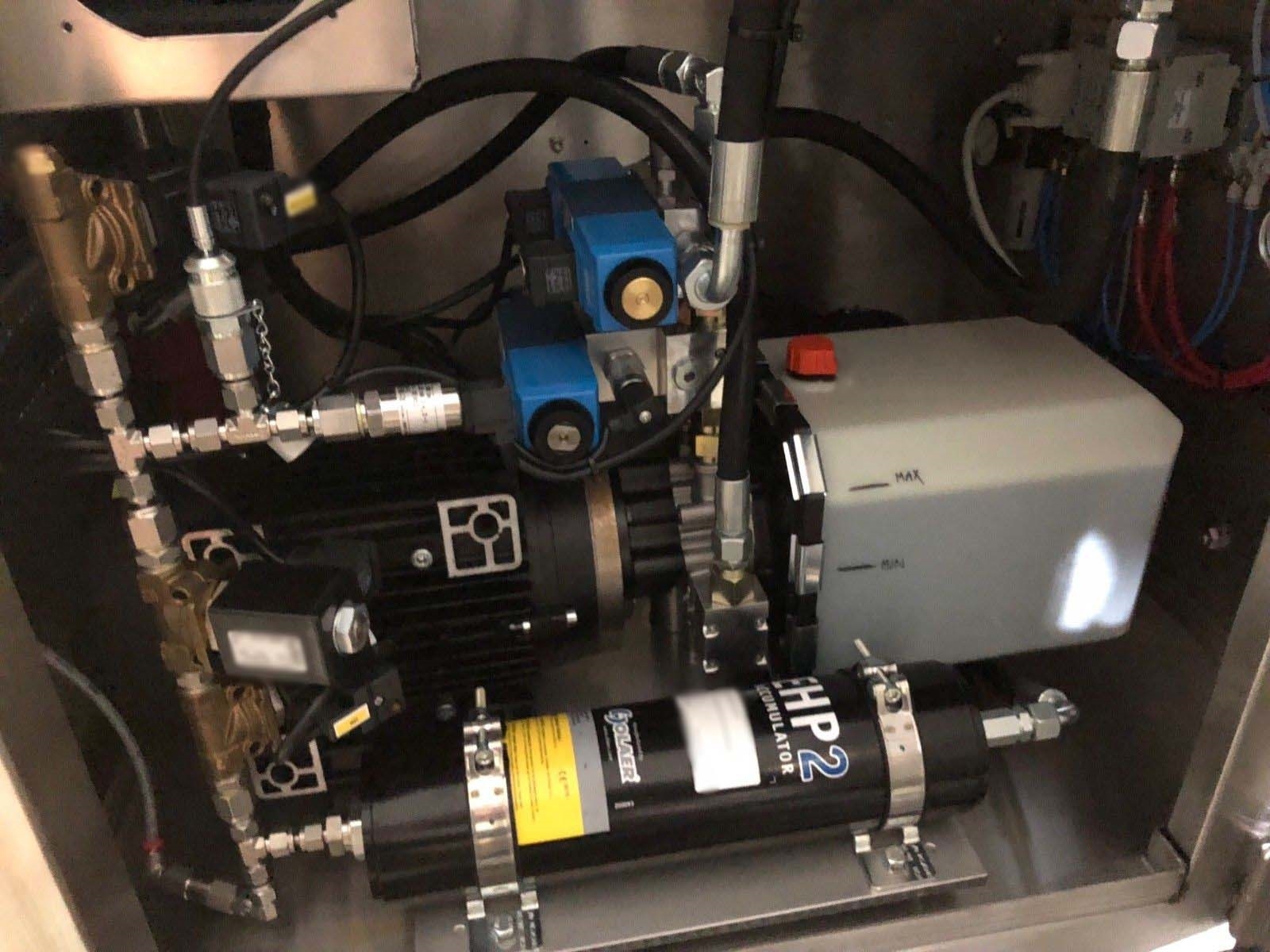
Nano Imprint Lithography (NIL) system, 6"
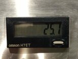
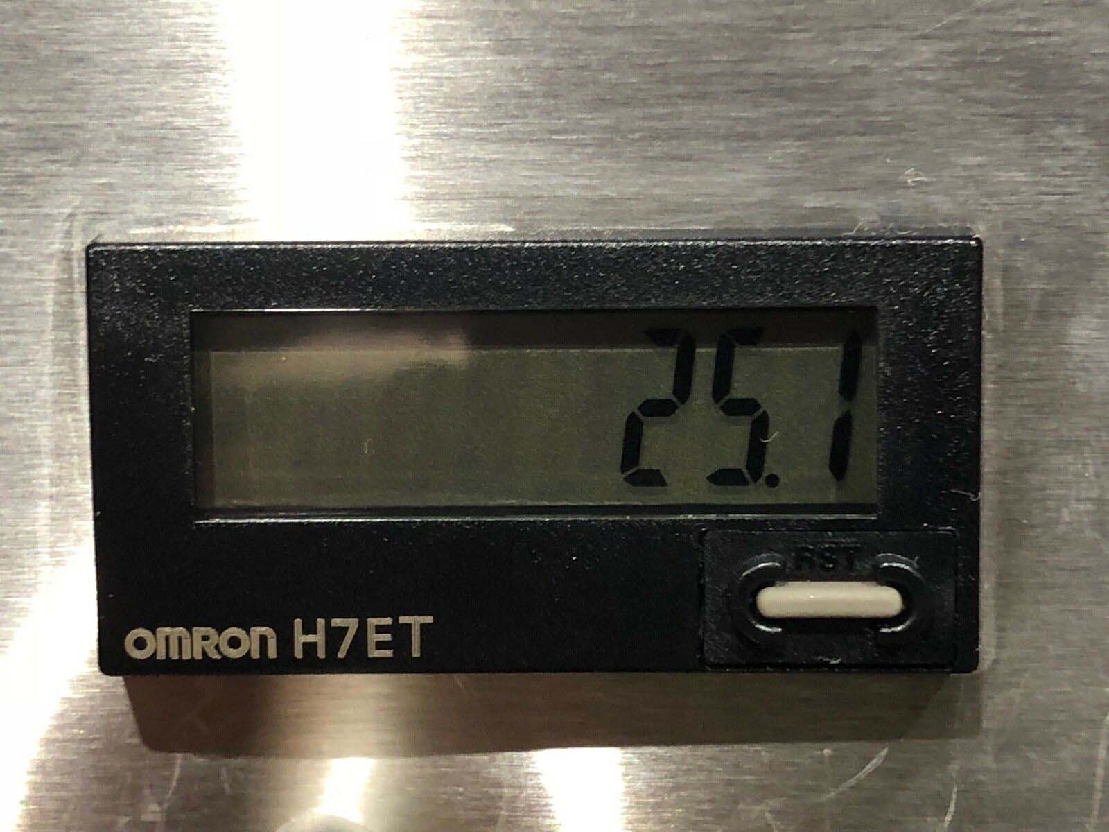
UV hour meter: 25.1 Hours
Includes:
Chiller
Power transformer
Power supply.
OBDUCAT Eitre 6 is a next generation inspection equipment offering comprehensive image quality control and defect classifications for both printed circuit board (PCB) devices and semiconductor mask and wafer devices. It is a dedicated equipment composed of various components which includes the imaging application, control electronics and defect classification software that applies the newest technologies and ideas. The system utilizes advanced vision technology and proprietary algorithms to ensure accurate detection of critical defects, enabling it to inspect critical layers for both PCB and wafer devices. The imaging application utilizes a high-magnification optical sensor to identify and measure very small defects. The sensor runs at a high speed and can capture line widths up to 1000 µm and heights up to 1000 µm with an accuracy of ±1 µm. The control electronics consists of an advanced motion controller coupled with an extremely precise linear motor unit. The motor machine has been designed to offer accuracy and speed, allowing it to scan the inspected area quickly and accurately. The tool covers a wide range of vision applications due to its reliable and robust imaging technology. The defect classification software is equipped with learning capabilities and a set of customizable parameters that enable the asset to automatically recognize defects. It uses a library of templates and parameters to quickly recognize and classify defects. Eitre 6 uses a sophisticated defect detector to help identify the most important defects and defect-like features. This helps to increase the accuracy of the defect classification. The detector runs at high speed and can identify almost any type of defect with a low false negative and false positive rate. The overall benefit of using OBDUCAT Eitre 6 is that it eliminates the need for manual inspection. This reduces the risk of human error, which can lead to significant cost savings. Additionally, it can be used for many different types of mask and wafer inspection applications, ranging from surface profiling to wafer-edge scans. Its simple user interface and high level of automation makes it easy to set up and use and ensures high-quality results.
There are no reviews yet

