Used PARAGON Ultra 200 #9203540 for sale
URL successfully copied!
Tap to zoom


ID: 9203540
Laser imaging system
Minimum pitch: 20µm
Minimum feature size: 8µm
Data resolution: 1µm (25,400 dpi)
Edge roughness (3σ): ±1µm
Registration accuracy (FTG): ±5µm
Side to side registration (3σ): 10µm
Maximum substrate size: 558mm x 660mm 22" x 26"
Maximum image size: 508mm x 609mm 20" x 24"
Substrate thickness: 0.05mm to 3mm
Imaging wavelength: UV range, 355nm
Energy range: 10-2200 mJ/cm²
Different energy settings:
500 x 400mm, 4 Symmetrical targets, 6sec load/unload
10mJ/cm² - 34 panels/hour
80mJ/cm² - 34 panels/hour
100mJ/cm² - 30 panels/hour
120mJ/cm² - 25 panels/hour
Applications:
IC Substrates
Solder mask
Inner layers & outer layers
Sequential build-up layers
Flex & rigid-flex PCBs
Standard configuration:
Laser system
OPFX Input
RIP Server
8GB Raster memory
Scaling system & power vacuum
System options:
Hole-free inner layer registration
Partial scaling
Wise scaling
Stamping
2D Barcode stamp
Additional vacuum customization plate.
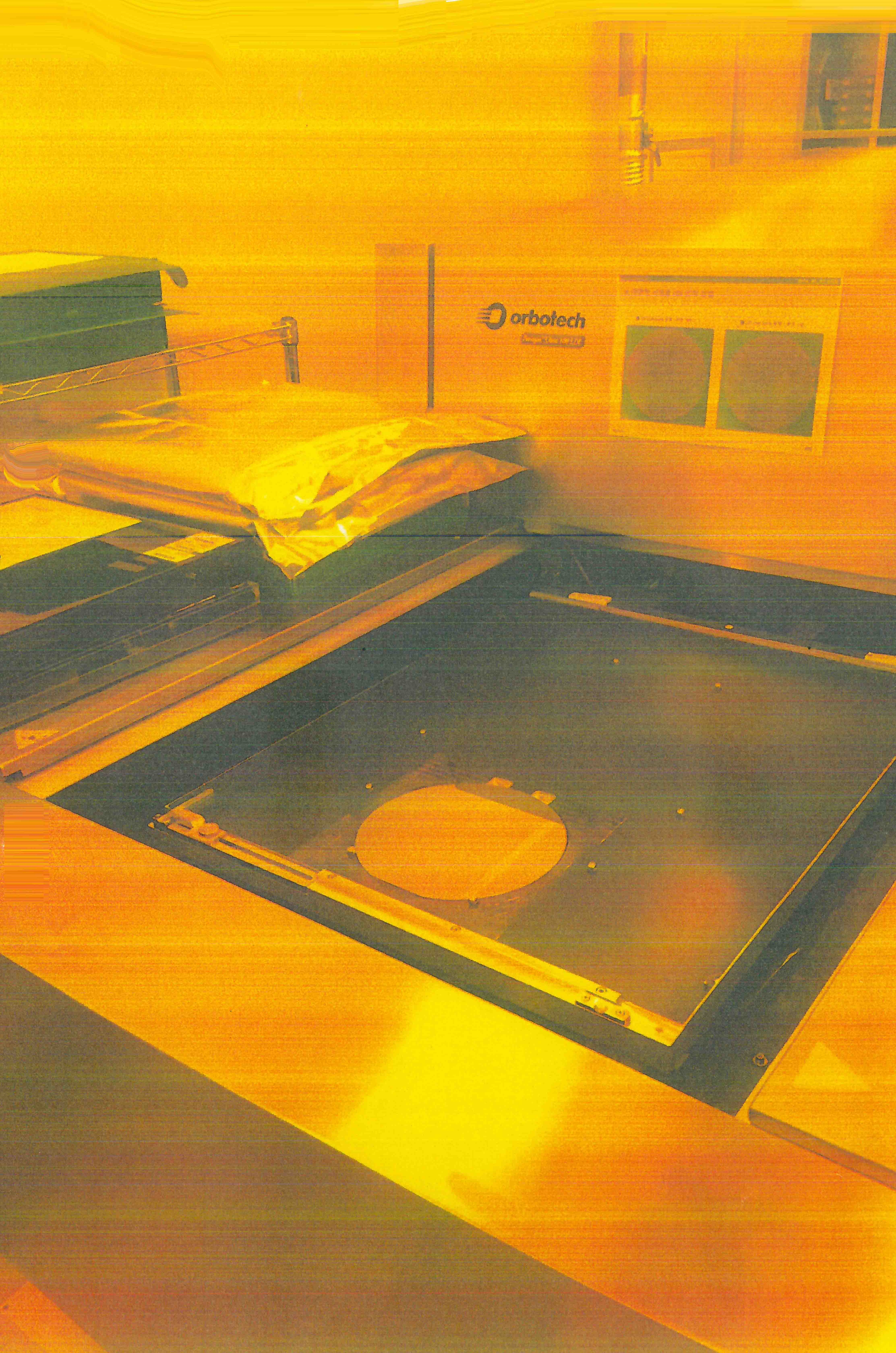
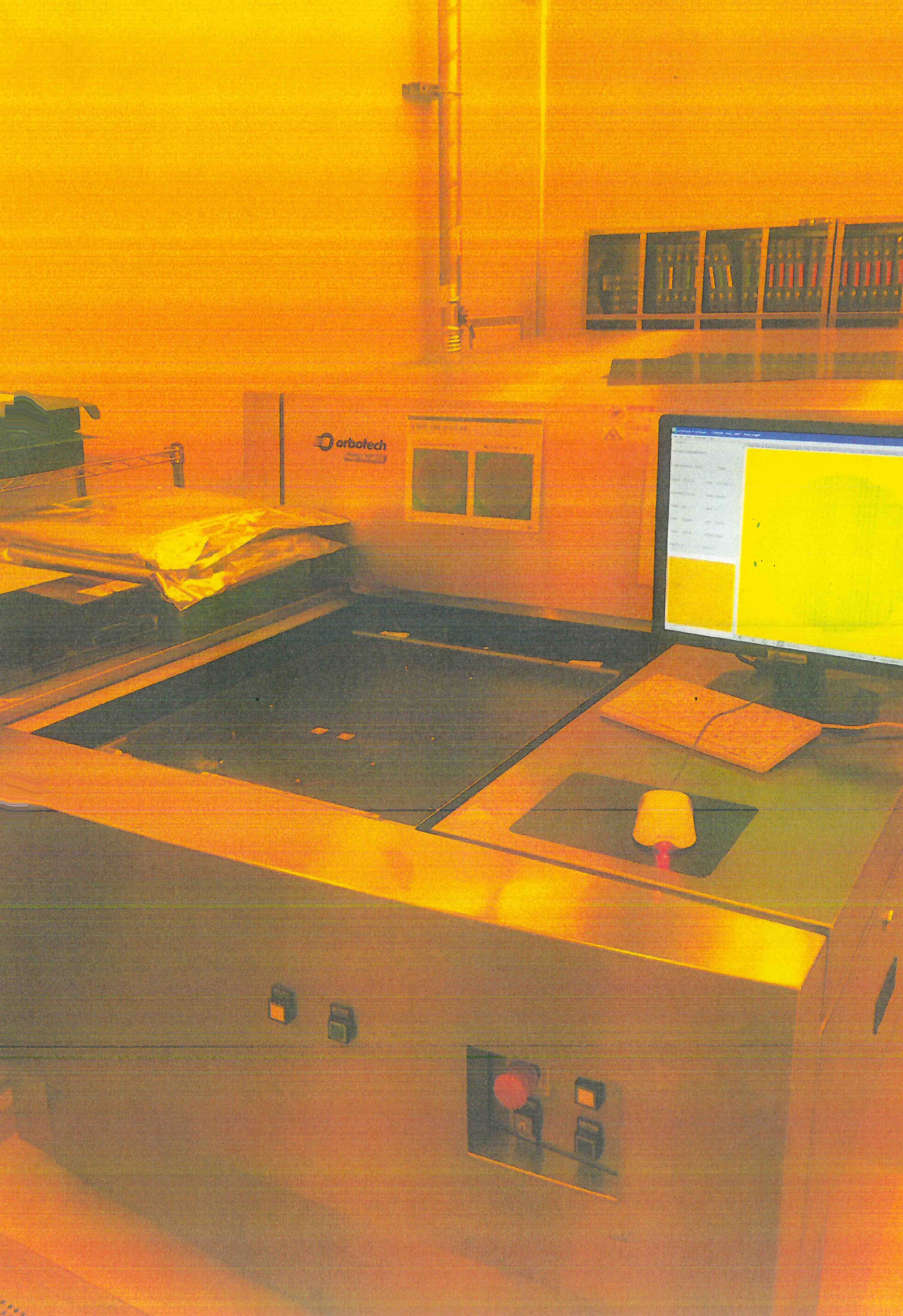
PARAGON Ultra 200 is a mask and wafer inspection equipment designed for accurately inspecting and measuring device features on semiconductor wafers. This system helps manufacturers meet high-level industry standards for yield and quality. The unit features a hybrid illumination machine, which has an adjustable back light to ensure accurate optical inspections across a wide range of semiconductor wafers. With this tool, manufacturers can perform more accurate inspections by adjusting the intensity of the light to match the refractive index of the wafer. Ultra 200 also features a 7 megapixel camera and advanced image processing algorithms, which ensure high-resolution detection and allow users to detect defects as small as 0.5 microns. The asset also has specialized software to analyze the scanned images and highlight potential defects. The model is capable of capturing images of two-dimensional (2D) and three-dimensional (3D) semiconductor devices, and supplies accurate process-specific information that can then be used for further analysis. In addition, the equipment can be used to analyze optical properties such as reflectivity, polarization, diffuse light, and birefringence. The system is also equipped with advanced calibration algorithms, which enable automated calibration of the imaging unit without user intervention. This ensures that the machine remains compliant with industry standards and gives the user accurate results. For manufacturing companies that wish to maintain the highest levels of quality, PARAGON Ultra 200 provides a reliable and accurate tool for mask and wafer inspection. The asset is highly reliable, with a high level of accuracy and precision. This allows users to detect defects with ease while also ensuring that their products meet industry standards.
There are no reviews yet


