Used PARAGON Ultra 60 #9203543 for sale
URL successfully copied!
Tap to zoom


ID: 9203543
Laser imaging system
Minimum pitch: 50µm
Minimum feature size: 16µm
Data resolution: 2µm (12,700 dpi)
Edge roughness (3σ): ±1µm
Registration accuracy (FTG): ±8µm
Side to side registration (3σ): 15µm
Maximum substrate size: 558mm x 660mm 22" x 26"
Maximum image size: 508mm x 609mm 20" x 24"
Substrate thickness: 0.05mm to 3mm
Imaging wavelength: UV range, 355nm
Energy range: 10-2200 mJ/cm²
Different energy settings:
500 x 400mm, 4 Symmetrical targets, 6sec load/unload
10mJ/cm² - 80 panels/hour
20mJ/cm² - 80 panels/hour
80mJ/cm² - 35 panels/hour
10mJ/cm² - 30 panels/hour
120mJ/cm² - 25 panels/hour
Applications:
IC Substrates
Solder mask
Inner layers & outer layers
Sequential build-up layers
Flex & rigid-flex PCBs
Standard configuration:
Laser system
OPFX Input
RIP Server
8GB Raster memory
Scaling system & power vacuum
System options:
Hole-free inner layer registration
Partial scaling
Wise scaling
Stamping
2D Barcode stamp
Additional vacuum customization plate.
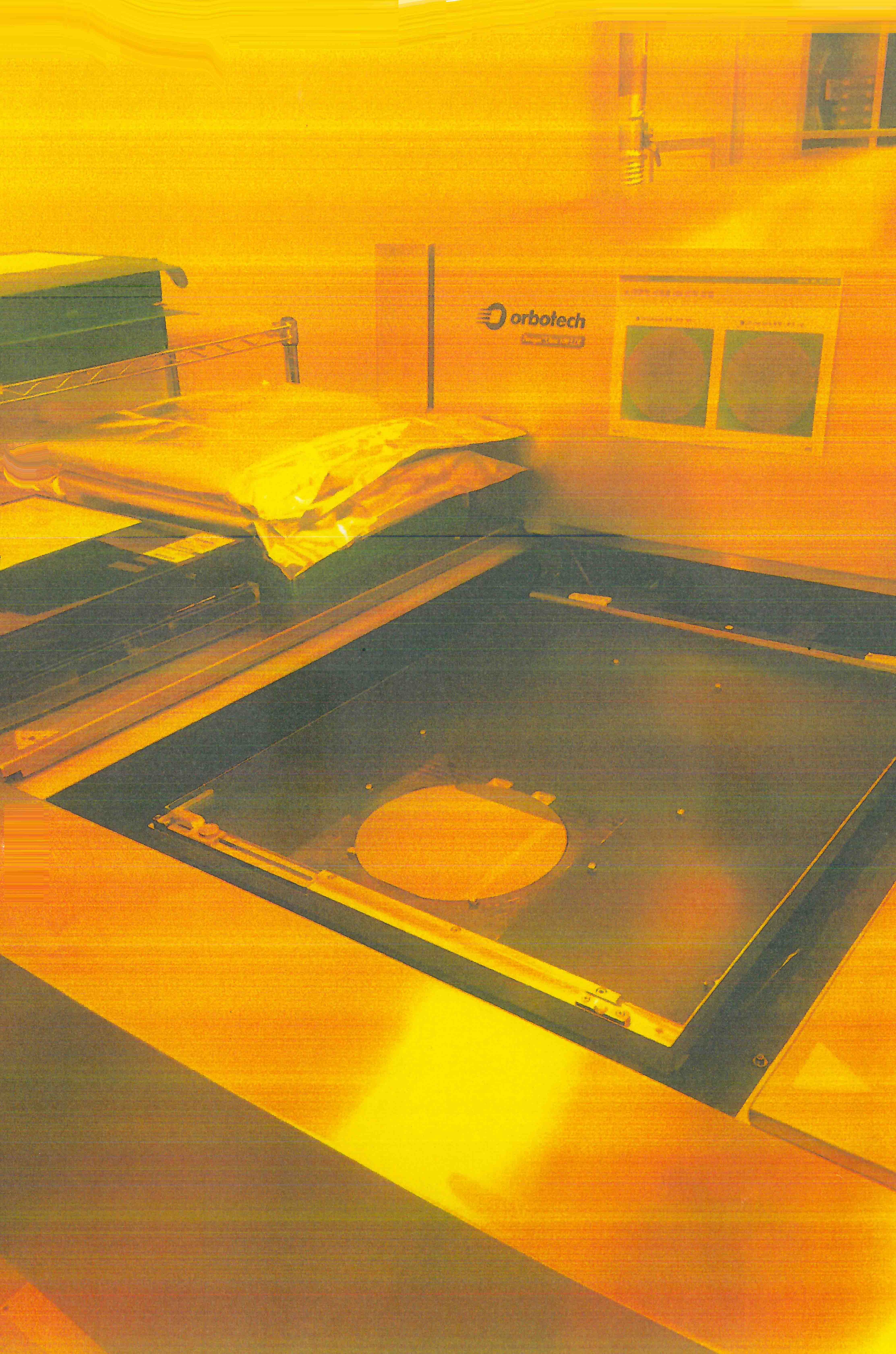
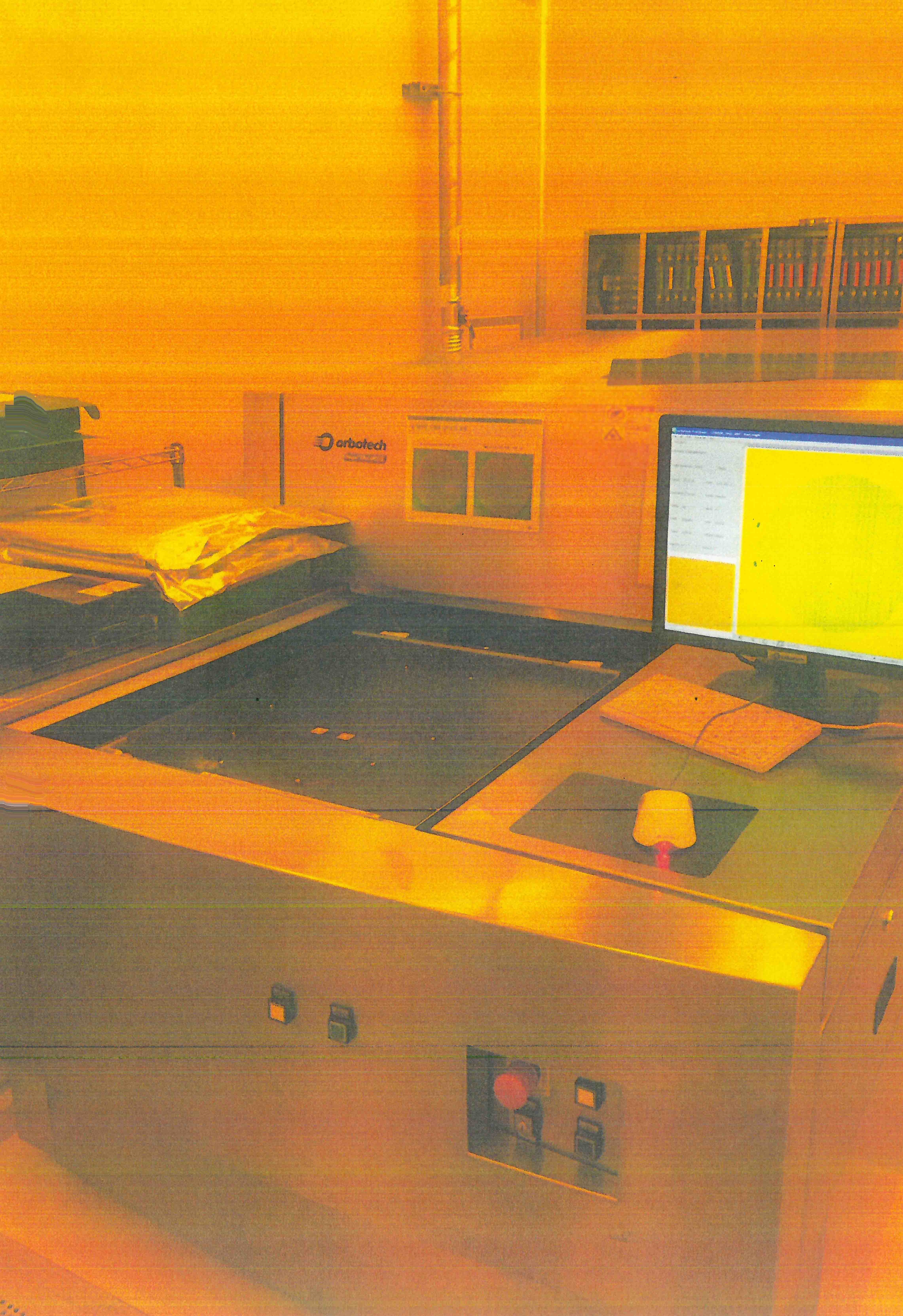
PARAGON Ultra 60 is a high-precision Mask & Wafer Inspection Equipment that offers advanced metrology with high performance yields. The system is specifically designed to inspect mask and wafer defects with high accuracy, reproducibility and repeatability. The unit can detect process-related defects, residue and out-of-specification features. The machine uses an advanced imaging technology that is capable of imaging both front and back sides of the mask and wafer. This enables the tool to measure features and defects accurately. The asset is also capable of performing critical detection and analysis of defects due to temperature variations, deposition and material resistance. The model uses accurate automatic defect inspection for both image and electrical measurements. This allows the equipment to accurately identify and measure defects due to process variations. The optical system is also capable of detecting small pattern defects, such as thin lines and/or other features with a tool resolution of less than 2nm. The unit also features a user-friendly graphical interface with intuitive control panels and ergonomic measure design. This provides easy operation and data interpretation, as well as multiple operating modes. Ultra 60 is equipped with an ultra-fast scan speed of up to 500mm/s, allowing for rapid detection and analysis of defects. The machine is also compatible with various formats like SEMI P-O or other standard formats. The tool is capable of operating in a dry or wet environment, making it suitable for a wide range of applications. The asset also offers a wide field-of-view to facilitate defects to be detected and measured. Its user-friendly control panel includes a standard user interface for easy data communication. It also includes a built-in set of comparison algorithms that can detect missing structures, printing defects, misalignments and missing channels on a 3D image of the mask or wafer. PARAGON Ultra 60 is designed to work with a variety of diagnostic tools, including contact and non-contact techniques. It is also capable of measuring process or material related defects with high accuracy. In conclusion, Ultra 60 is highly efficient and reliable Mask and Wafer Inspection Model that offers advanced metrology with high performance yields. Its user-friendly control panel and wide field-of-view offer ease of use, making it suitable for a variety of applications.
There are no reviews yet


