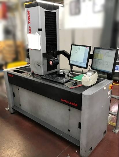
Used PARLEC P2500A-0387 #9266043 for sale
URL successfully copied!
Tap to zoom


PARLEC P2500A-0387 is a high-precision Optical/Scanning Electron Microscope (SEM) and Mask & Wafer Inspection Equipment. This system allows its users to view and measure the critical pattern features of masks and wafers at the nanometer-level. P2500A-0387 has a high-resolution SEM imaging unit, which enables users to view and measure fine pattern features. It is equipped with an advanced automatic wafer scanning capability, which can be used to automagically map the entire wafer. Its automatic feature extraction capabilities can accurately detect and measure defects, characterization of overlay data, and feature analysis. The machine is able to inspect a wide range of masks and wafers, ranging from advanced process nodes to low-k dielectric layers. Furthermore, this tool features convenient user interfaces, so users are able to interact with the data quickly and efficiently. PARLEC P2500A-0387 utilizes optical imaging process for fine feature measurement. By taking advantage of spread spectrum interferometry, edge contrast, and non-destructive IR imaging, PARLEC is able to measure surface topography with high accuracy and precision. The IR imaging process can detect and measure low-k material thickness, which is critical for advanced process nodes. The SEM imaging asset includes secondary electrons, backscattered electrons, and X-ray detectors. All of these detectors can be used for measuring both feature shape and dimensional parameters. Furthermore, users have access to a wide range of specimen rotation capabilities, which enable them to accurately measure 3D topography of difficult features. The Mask & Wafer Inspection Model has powerful interface software, which provides users with all the necessary parameters for wafer measurement and analysis. It also supports a wide range of powerful automation tools, including edge detection, feature analysis, and overlay measurements. Overall, P2500A-0387 is an extremely powerful and accurate Mask & Wafer Inspection Equipment. It is designed to enable users to measure critical pattern features at the nanometer-level, and it is capable of taking full advantage of advanced process nodes and low-k dielectric layers. Furthermore, its highly interactive user interfaces and automated features make this system an invaluable device for any EMS laboratory.
There are no reviews yet