Used SEMICONDUCTOR DIAGNOSTICS FAaST 350 #293820125 for sale
URL successfully copied!

Tap to zoom

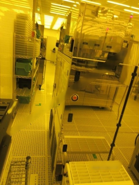
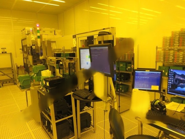
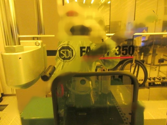
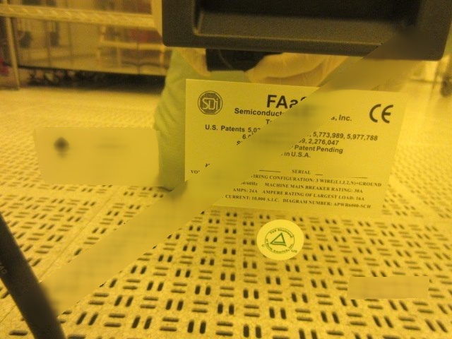
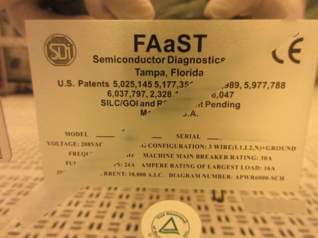
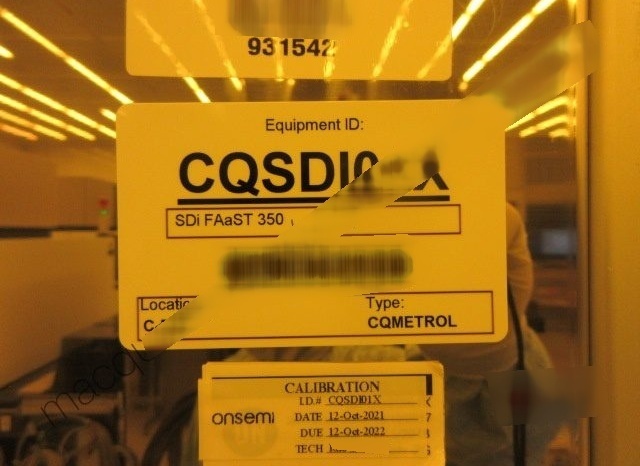
ID: 293820125
Wafer Size: 8"
Vintage: 2006
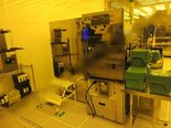
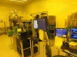
Semiconductor diagnostics system, 8"
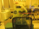
FAAST Electrical diagnostics platform
Probe diagnostics
Surface photovoltage
Capacitance‑voltage measurement capabilities
2006 vintage.
SEMICONDUCTOR DIAGNOSTICS FAaST 350 is a cutting-edge mask and wafer inspection equipment designed to meet the rigorous demands of semiconductor manufacturing. This advanced system combines state-of-the-art technologies to enable high-speed and high-accuracy inspection of masks and wafers used in semiconductor fabrication processes. FAaST 350 unit is equipped with sophisticated imaging capabilities that allow for the detection and analysis of defects on masks and wafers with exceptional precision. It utilizes a combination of optical and electron beam technologies to capture detailed images of the samples under inspection, enabling the machine to identify defects at the nanoscale level. One of the key features of SEMICONDUCTOR DIAGNOSTICS FAaST 350 tool is its automated inspection capabilities, which streamline the process of defect detection and analysis. The asset is equipped with advanced algorithms and image processing techniques that enable rapid defect identification and classification, helping semiconductor manufacturers improve yield and ensure the quality of their products. FAaST 350 model is designed to inspect a wide range of semiconductor materials, including silicon wafers, photomasks, and other substrates used in the production of integrated circuits. Its versatility makes it an ideal solution for semiconductor manufacturers working on cutting-edge technologies such as advanced logic devices, memory chips, and sensors. In addition to defect detection, SEMICONDUCTOR DIAGNOSTICS FAaST 350 equipment also offers comprehensive analysis and reporting capabilities. Users can access detailed reports that provide insights into the types and locations of defects detected during the inspection process, helping them understand potential sources of variability in their manufacturing processes. FAaST 350 system is equipped with advanced software tools that enable users to customize inspection parameters, define defect criteria, and optimize inspection workflows according to their specific requirements. This flexibility allows semiconductor manufacturers to adapt the unit to different process nodes, material types, and defect types, ensuring that they can address the unique challenges of their manufacturing operations. SEMICONDUCTOR DIAGNOSTICS FAaST 350 machine is designed with scalability in mind, allowing semiconductor manufacturers to expand their inspection capabilities as their production volumes grow. The tool can be integrated into existing manufacturing lines and can accommodate increased throughput requirements without compromising on inspection accuracy or speed. Overall, FAaST 350 is a powerful and versatile mask and wafer inspection asset that offers semiconductor manufacturers a comprehensive solution for ensuring the quality and reliability of their semiconductor products. Its advanced imaging technologies, automated inspection capabilities, and customizable features make it a valuable asset for semiconductor manufacturing facilities looking to achieve high yields and consistent product quality.
There are no reviews yet