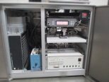
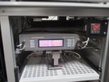
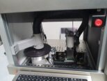
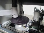
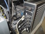
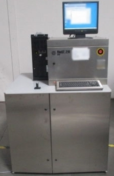
Used SEMILAB / SDI FAaSt 210E-SPV #9203133 for sale
URL successfully copied!
Tap to zoom







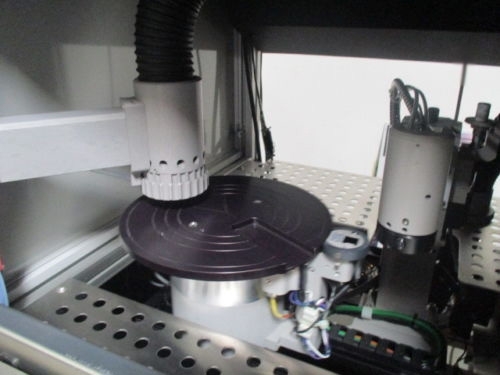

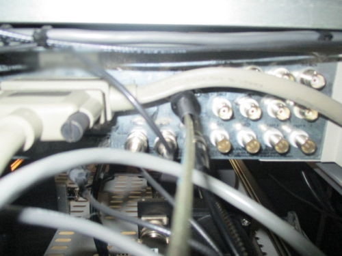


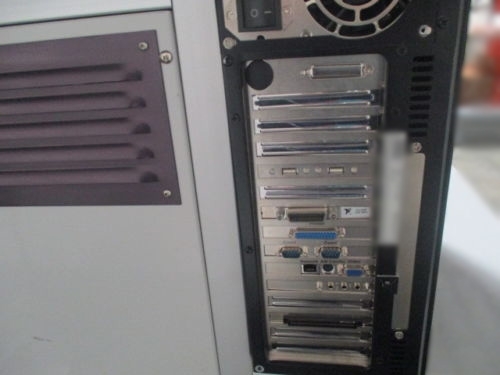



ID: 9203133
Wafer Size: 6"-8"
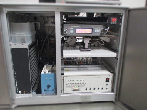
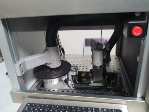
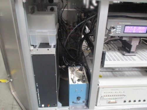
Contamination measurement system, 6"-8"
Unislide rotary table B4818TS
NEWPORT MM3000 + 23556
AD TECHNOLOGY 3800-1745
PHOTON Wheel BO76
SPV Lightsource
SIGNAL RECOVERY 197 Light chopper
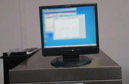
PLANAR PL100M
ADEK R7IFI48AB
PC700 Monster power center
Trip lite power production
Astrodyne MSCA-5005
API Getty 230-6102FH
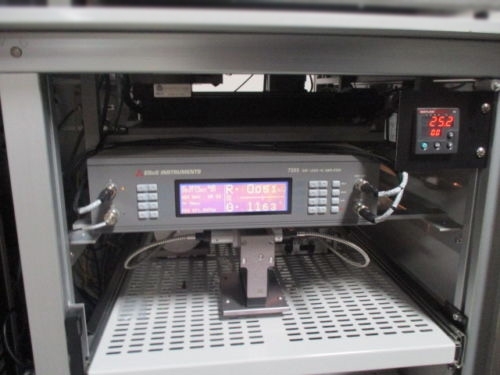
EG&G INSTRUMENTS 7265
TEXAS INSTRUMENTS Peripherals DT-5K-PS/2
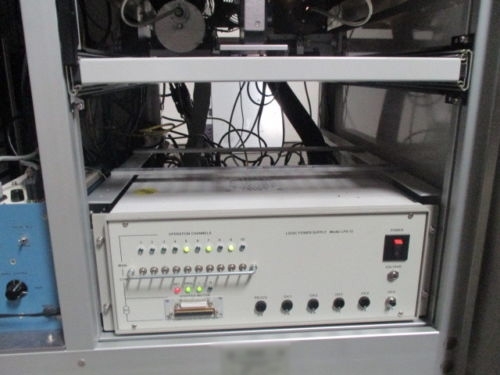
Logic supply power LPS-12
WATLOW 96
DANAHER 1122317
MG Chemicals 846-80G
Manuals not included
Power supply: 110 AC, 50/60 Hz, 3000 W.
SEMILAB / SDI FAaSt 210E-SPV is a medium-level mask and wafer alignment microscope equipment designed to inspect for defects, erosion, and surface integrity in semiconductor wafers and masks. This system features a built-in automated unit control (SC) with user-friendly intuitive graphical user interface (GUI). With an overall size of only 800 mm x 680 mm x 640 mm, this inspection machine is compact yet highly versatile. SDI FAaSt 210E-SPV offers a variety of features to empower operators in the semiconductor industry. This tool features a 10-position XYZ-stage that is capable of multi-layer inspection, automatic and manual stage alignment, tilt and wobble adjustment, and advanced autofocus capabilities. It also offers a brightfield/darkfield image display with direct-on-wafer operation, a 6 position condenser with 0.3-2.5X magnification range, and an up to 25X working distance. SEMILAB FAaSt 210E-SPV also provides image acquisition and analysis capabilities on various levels. With built-in imageshift correction, misalignment can be detected and accurately identified. It also includes an advanced algorithm-based feature identification and masking for defect-free inspection, edge detection, and particle count and size analysis. In addition, a wide variety of measurements can be taken including line width, edge profile, and overlay accuracy. Moving forward, FAaSt 210E-SPV is equipped with a high-resolution CCD camera asset, adjustable exposure time, and powerful PC-based image analysis model to generate an even greater range of defect/feature recognition and analysis. This equipment also includes a range of image reporting functions to evaluate results and view pass/fail status instantly. Overall, SEMILAB / SDI FAaSt 210E-SPV is a reliable medium-level mask and wafer inspection system designed to reliably detect and measure even the smallest defects. It offers a whole suite of advanced features to ensure users are able to get the best results out of their inspection process.
There are no reviews yet

