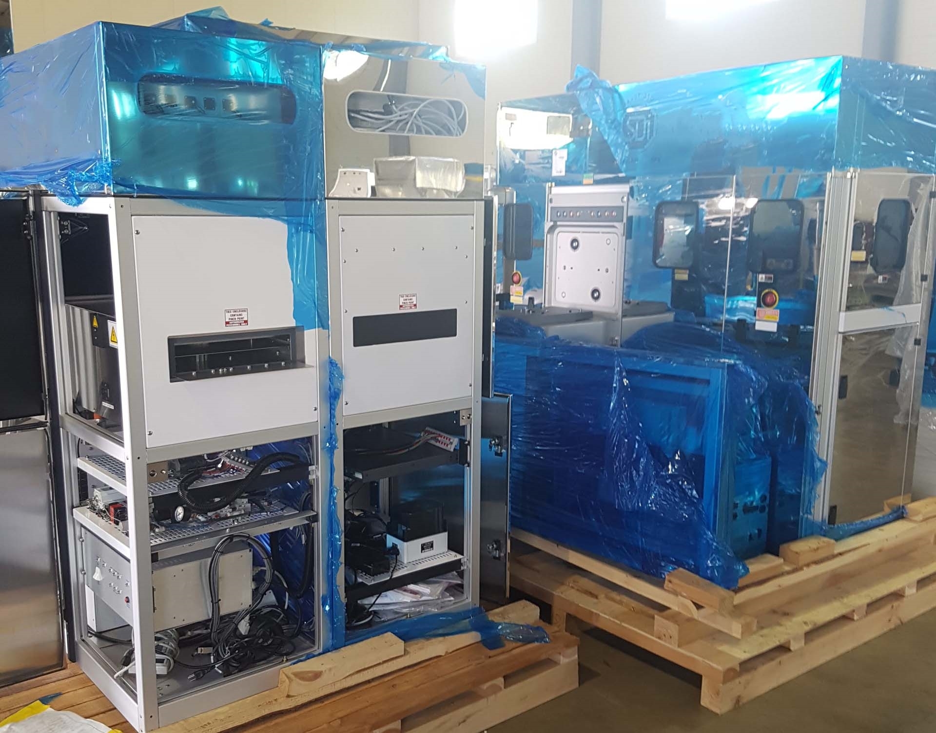
Used SEMILAB / SDI FAaSt 350 #9268262 for sale
It looks like this item has already been sold. Check similar products below or contact us and our experienced team will find it for you.
Tap to zoom


Sold
SEMILAB / SDI FAaSt 350 Mask and Wafer Inspection Equipment is designed for automated surface defect inspection of manufactured masks and wafers during the production of semiconductor integrated circuits. This automated system offers fast and reliable detection and evaluation of surface defects on a wide range of substrates, including wafers, masks, lead frames, electronic components, and other flat substrates. The unit includes the comprehensive SDI FAaSt 350 Optical Station, which is equipped with high-quality Leica optics for the highest precision imaging and defect detection. With its high resolution imaging capability, it can detect defects from as small as 4 μm, while its patented Low-FG illumination machine ensures a defect-free background image. This tool also provides excellent image contrast and visibility for easier defect identification and classification. SEMILAB FAaSt 350 is designed to be extremely user-friendly, with a simple and intuitive graphical user interface (GUI) allowing for quick and easy inspection of samples. Different settings can be programmed and saved on the asset, allowing the operator to quickly adapt the machine if the sample under examination requires a different inspection protocol. In addition to the imaging model, FAaSt 350 also features adaptive sub-resolution inspection algorithms that allow real-time detection and classification of defects. These algorithms analyse the images in order to accurately identify defects in the sample. Additionally, the machine's automated focus and contrast optimization Technologies provide accurate image capture to ensure accurate defect localization. SEMILAB / SDI FAaSt 350 equipment is also designed for high throughput operation, with its automated sample handling capabilities allowing up to 30 wafers per hour to be inspected. Its automated wafer alignment module easily accommodates a wide variety of wafer sizes and thicknesses, allowing for quick and easy wafer to wafer alignment. Once aligned, the system is capable of generating detailed quantitative results, allowing for greater confidence in defect detection. In conclusion, SDI FAaSt 350 Mask and Wafer Inspection Unit is an advanced automated machine designed specifically for the inspection of masks and wafers during the production of semiconductor integrated circuits. Its high resolution imaging capability, intuitive GUI, and advanced imaging algorithms provide highly accurate and reliable defect detection, while its throughput capabilities and automated sample handling make it an ideal choice for the high-speed inspection of manufactured samples.
There are no reviews yet