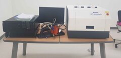
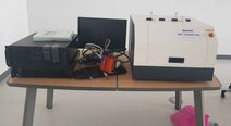
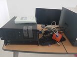
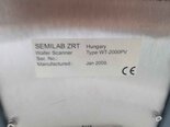
Used SEMILAB / SDI WT-2000PVN #293625326 for sale
URL successfully copied!
Tap to zoom


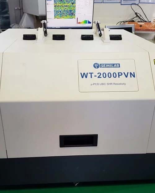

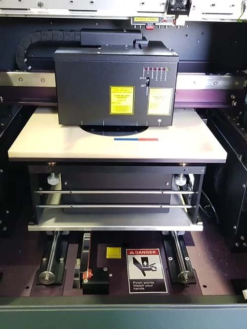

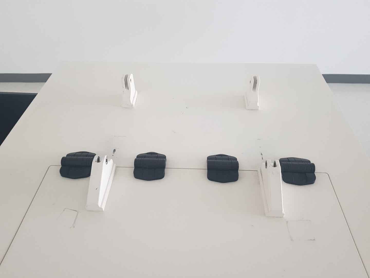

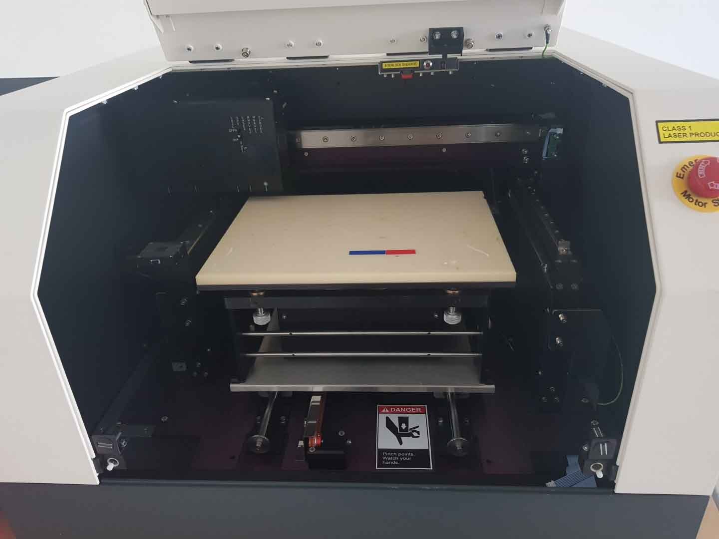

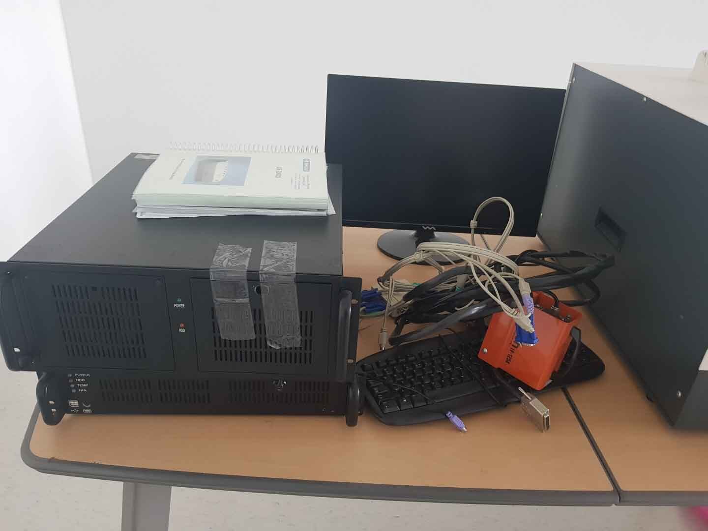

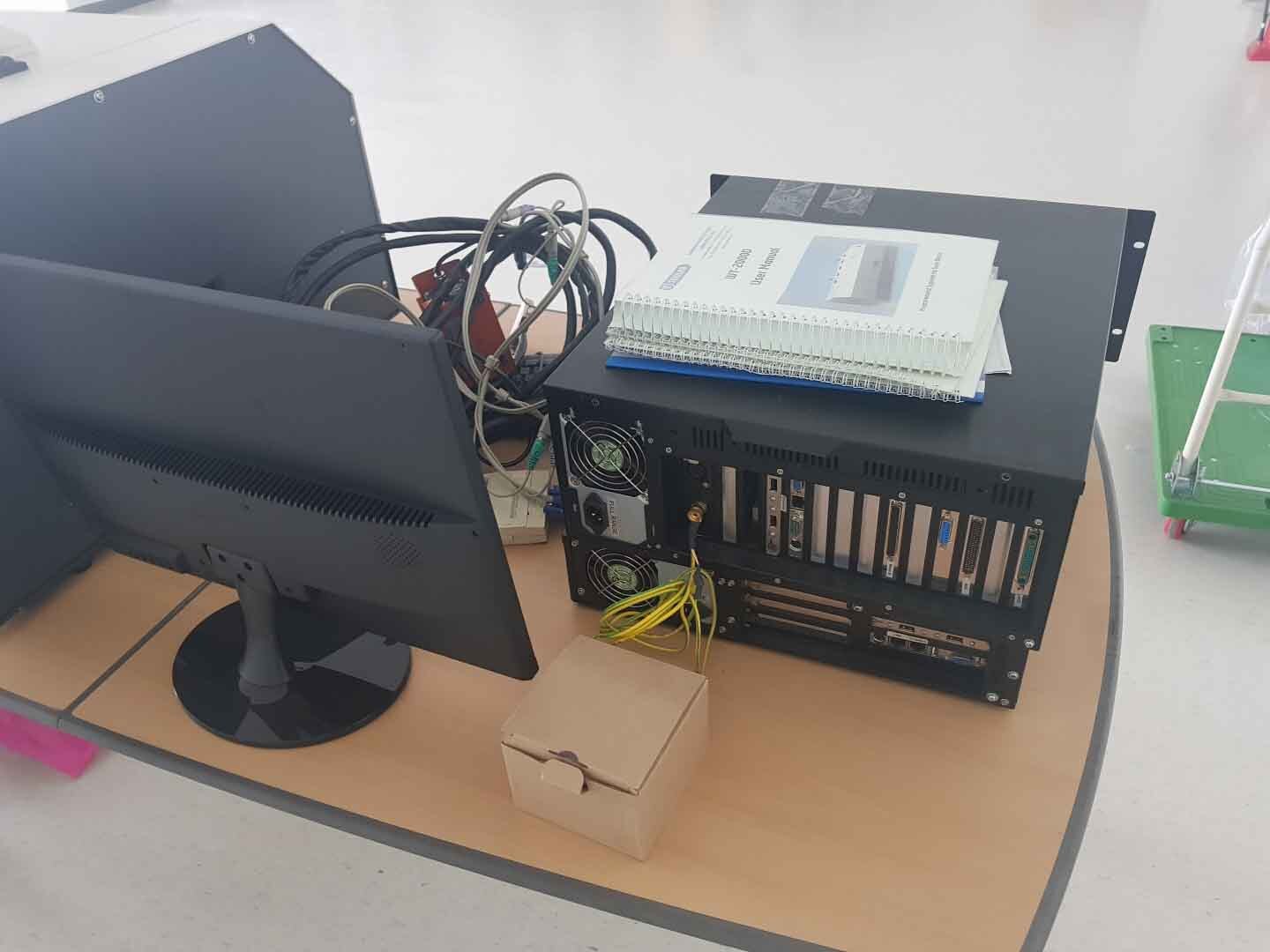

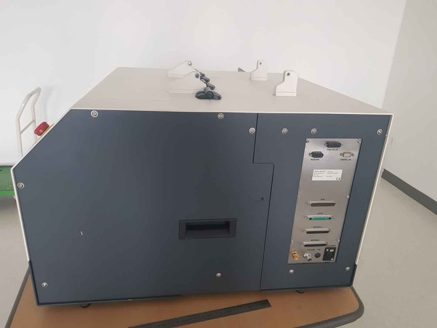

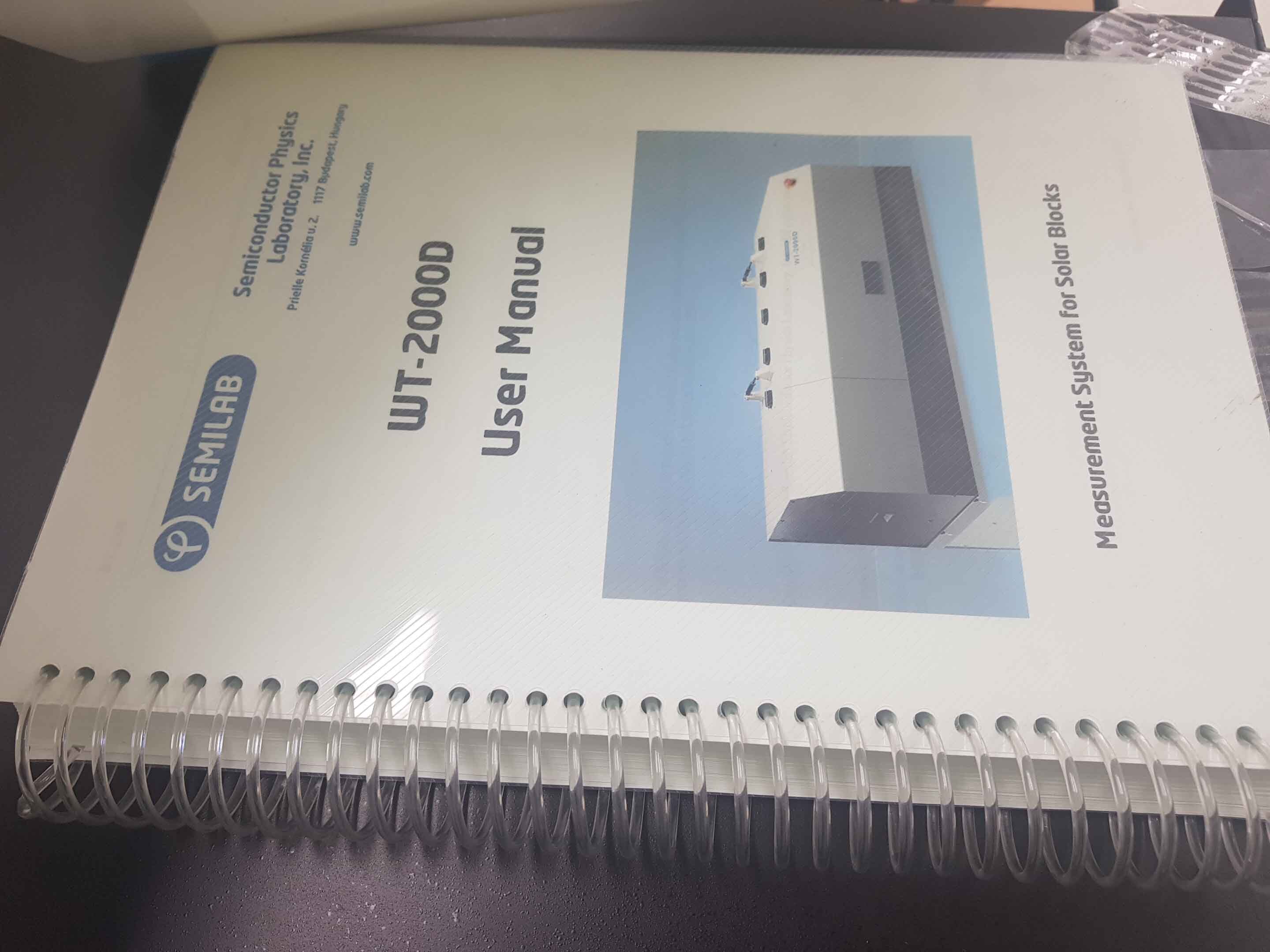

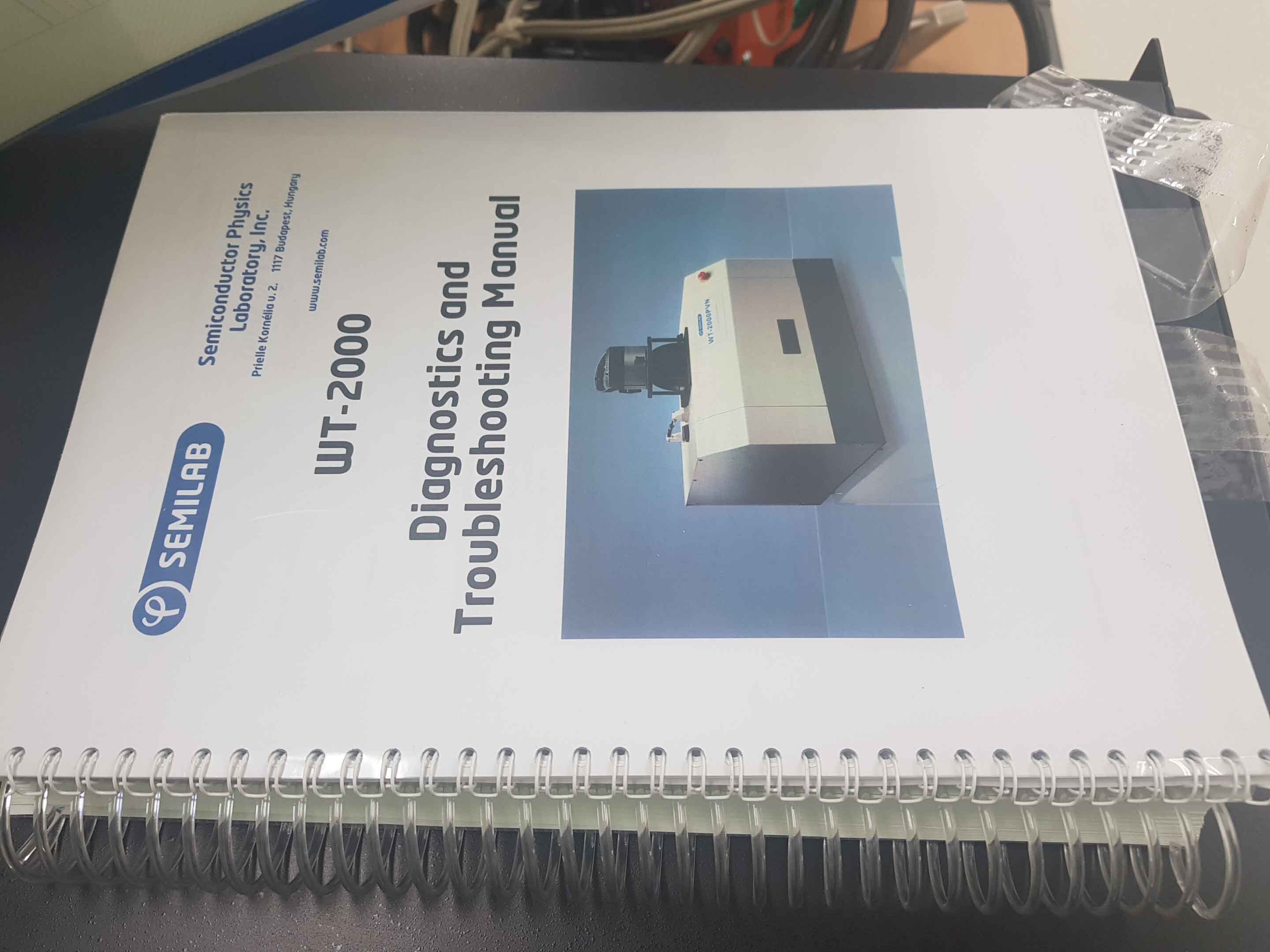


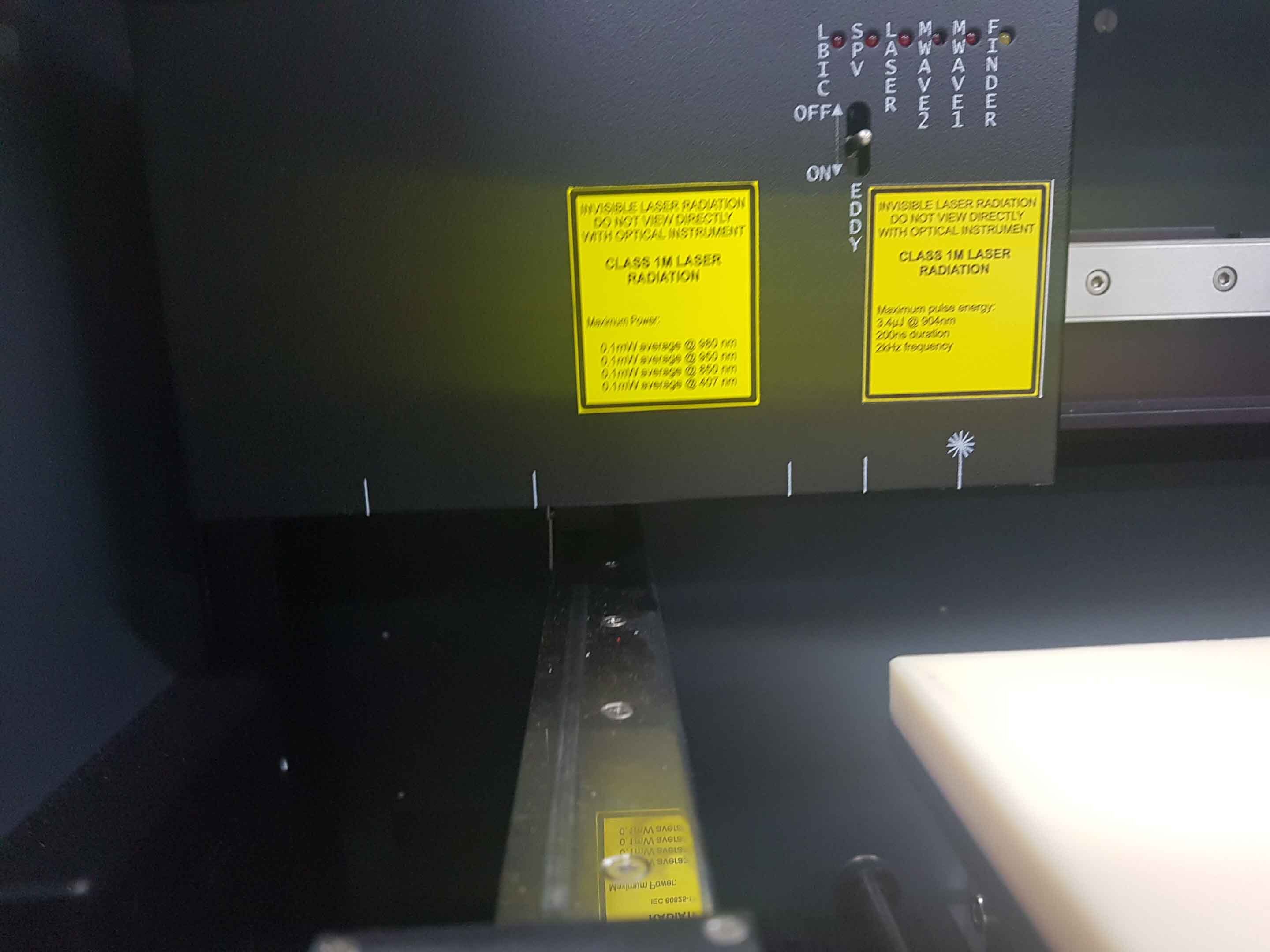

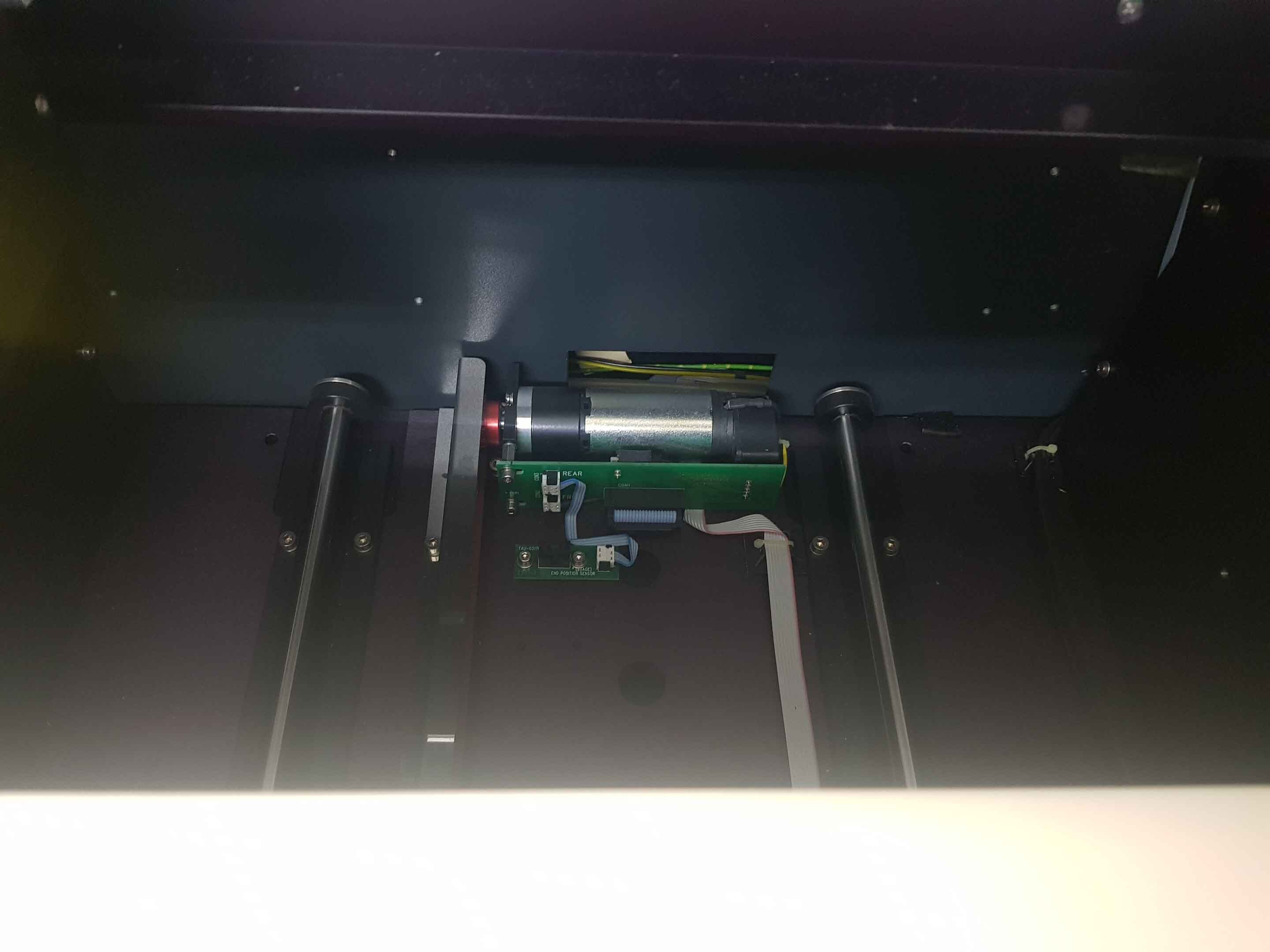

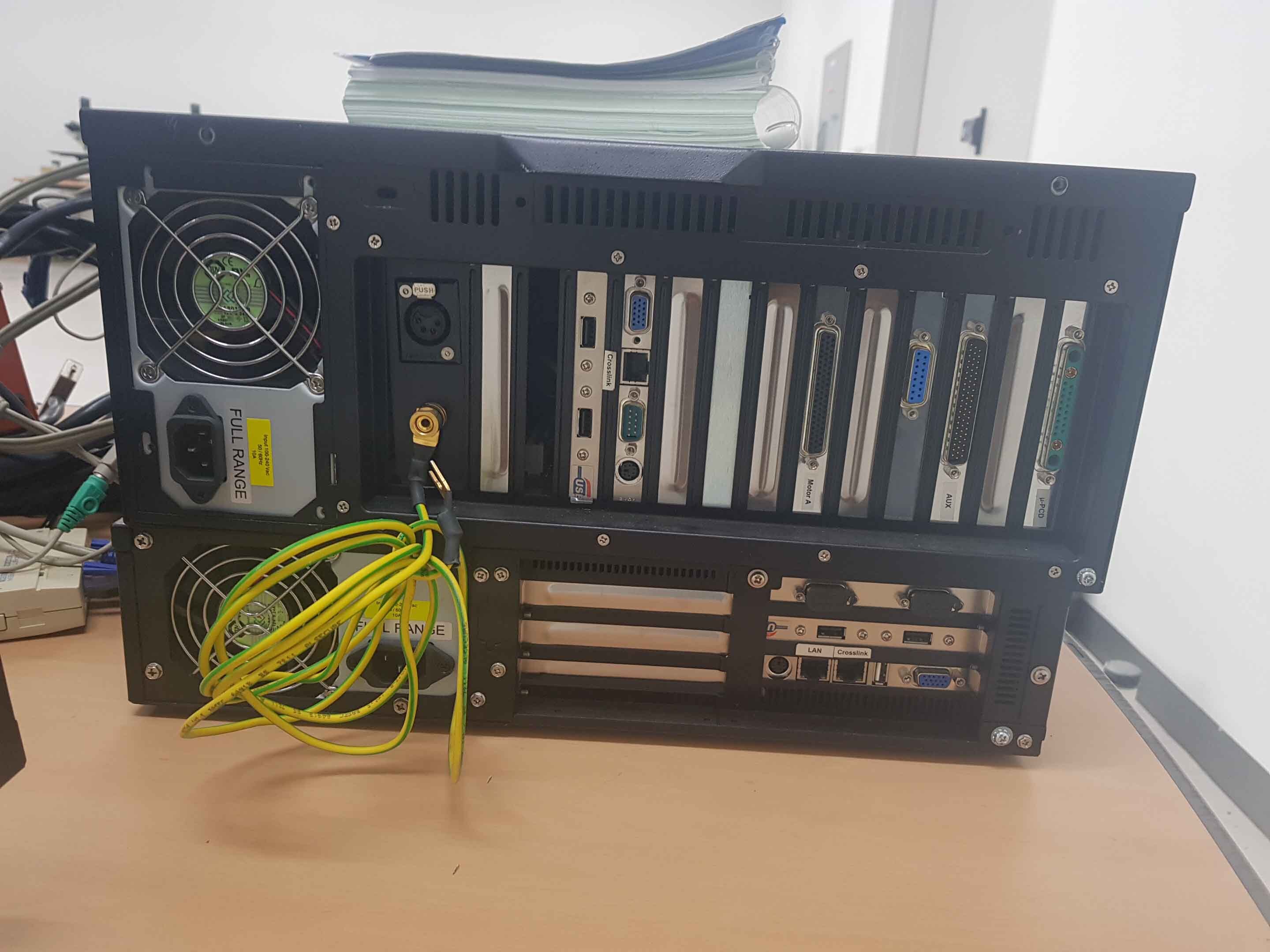

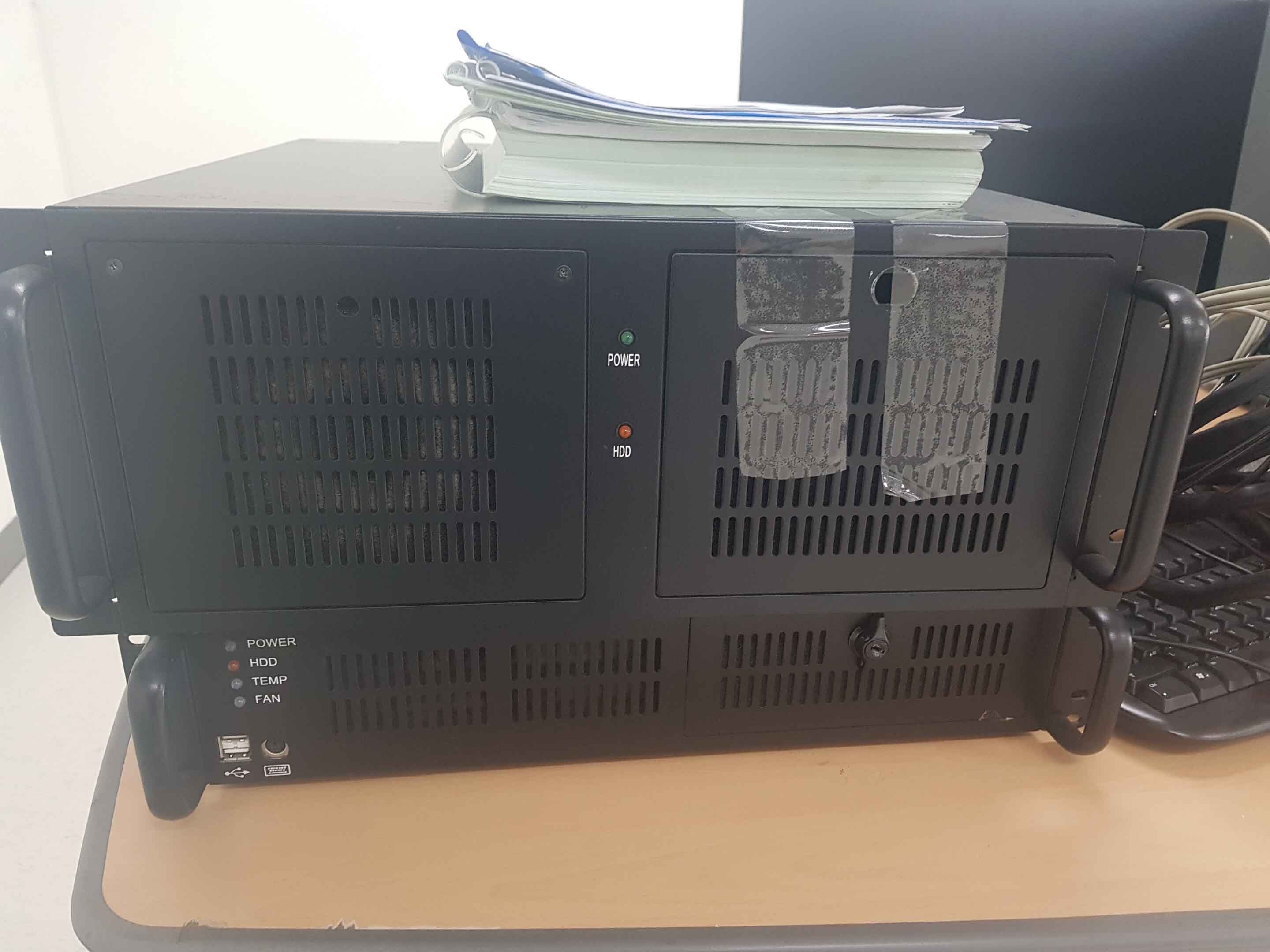

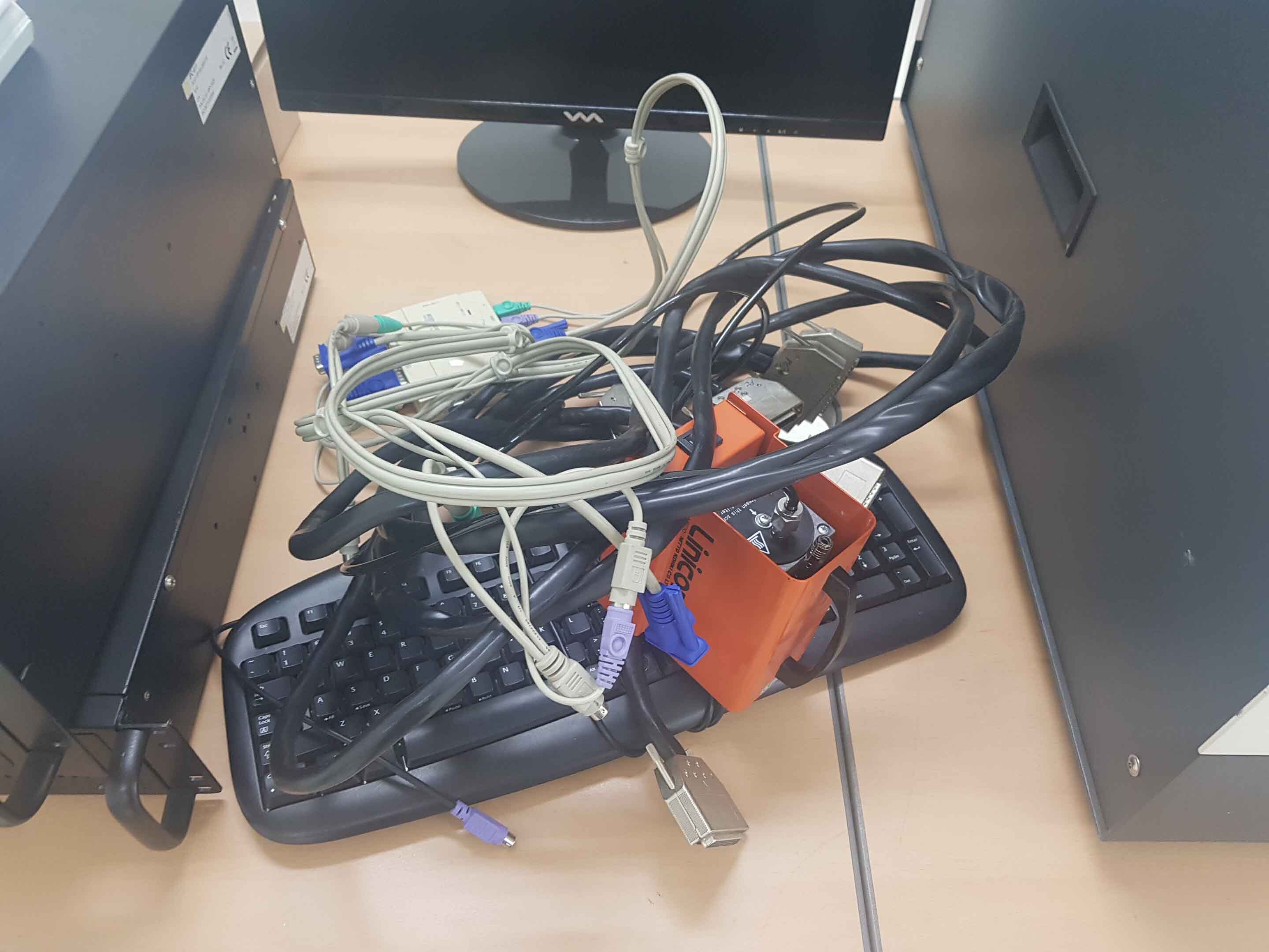

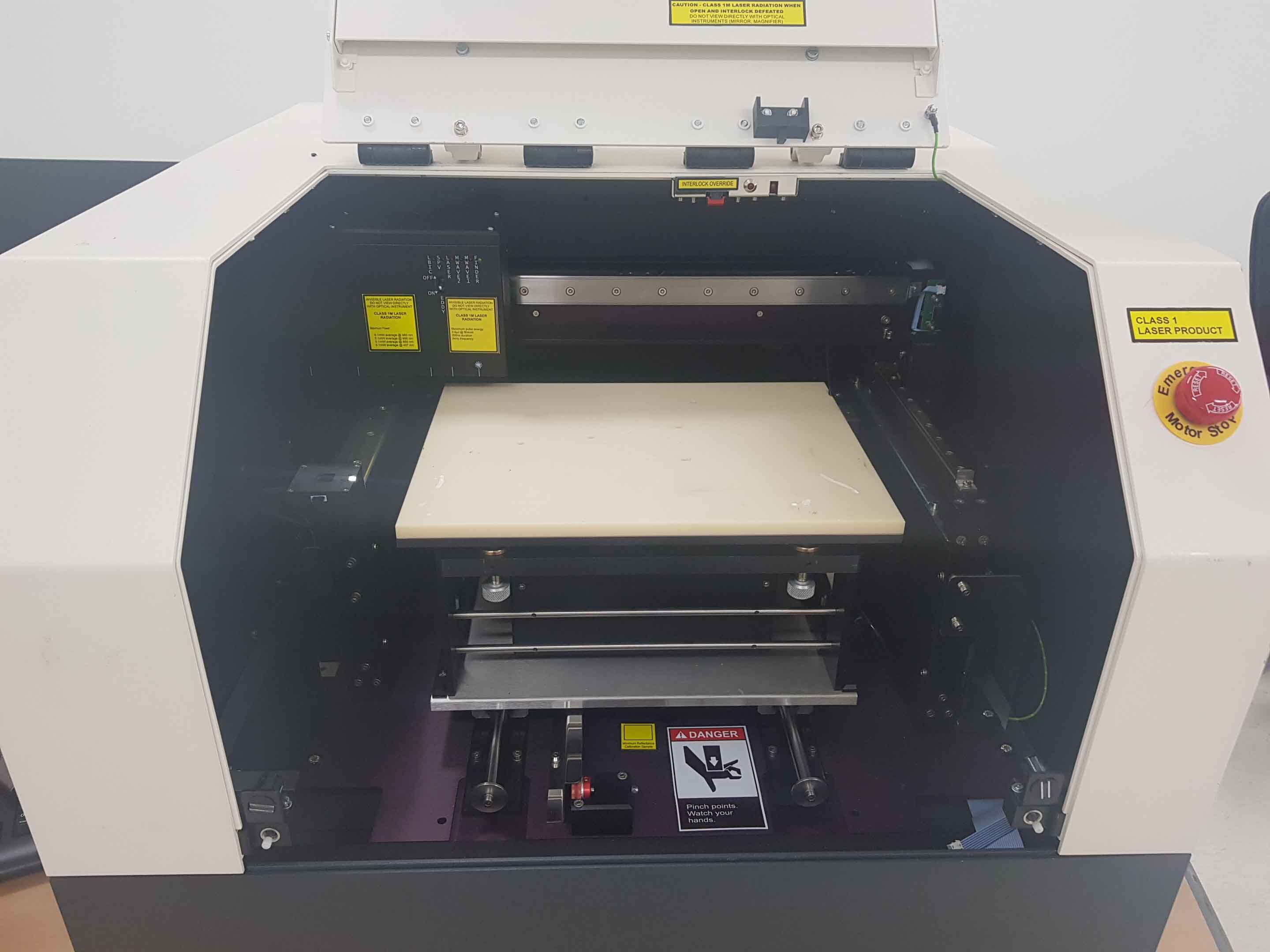

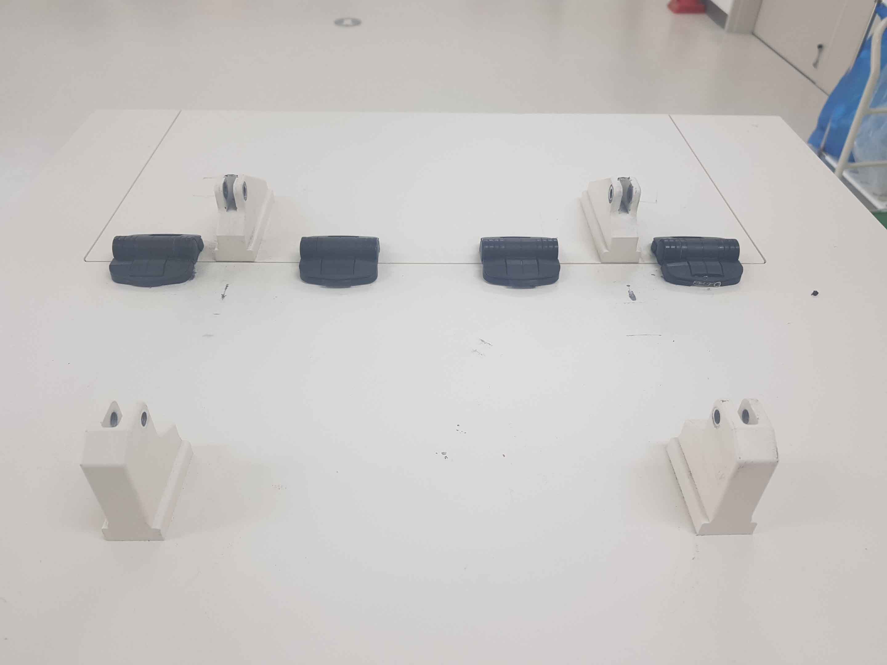

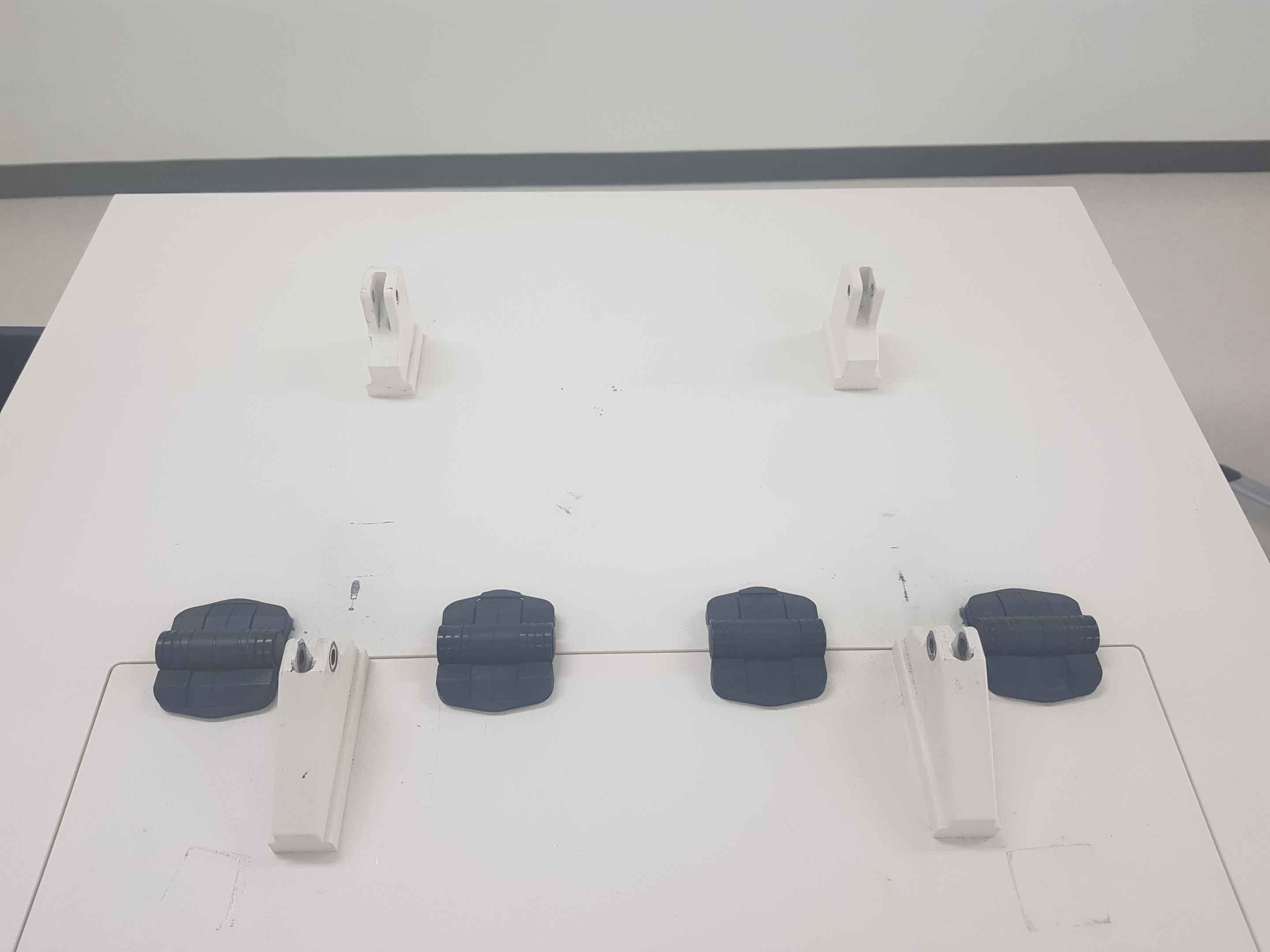


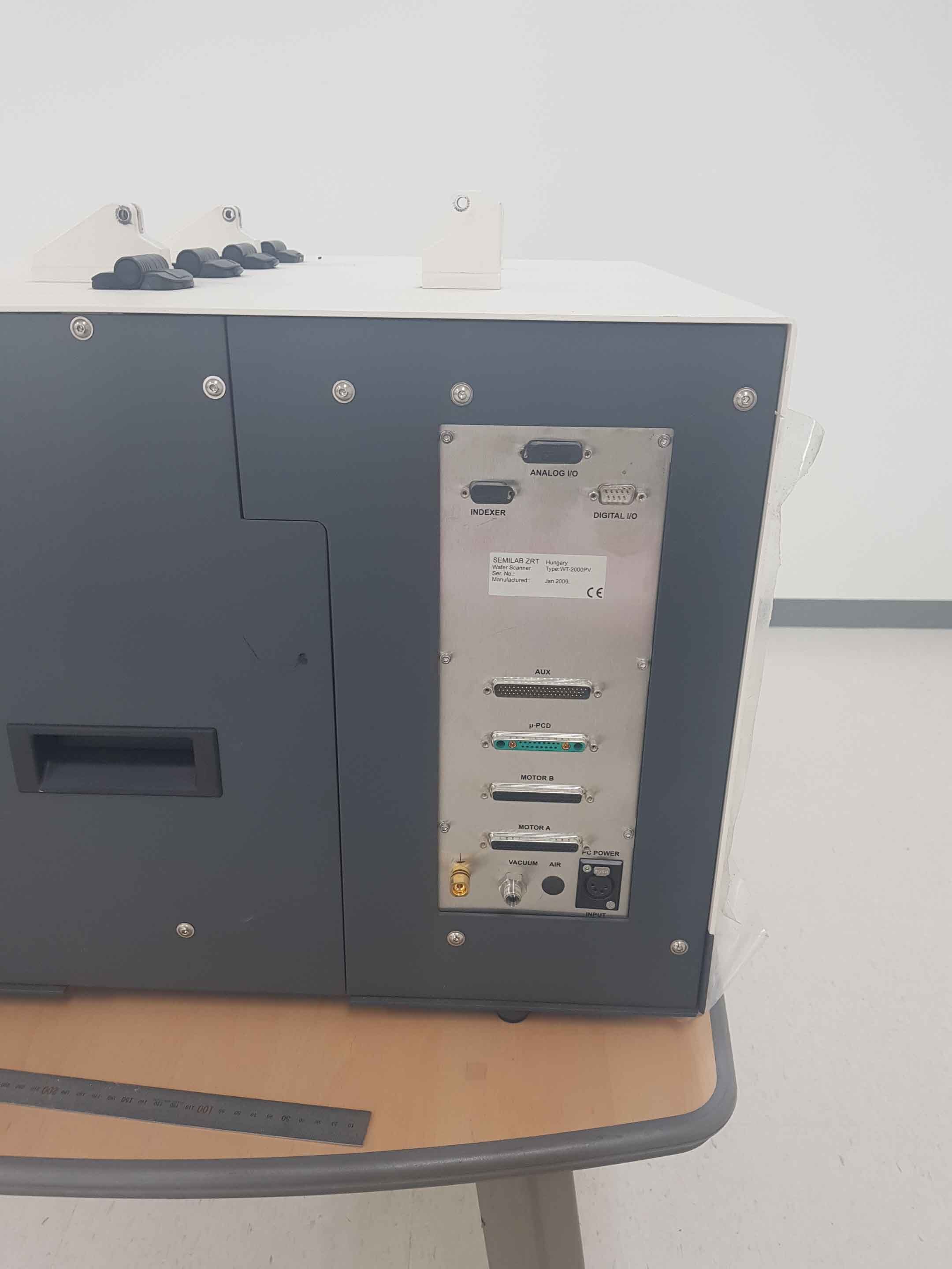

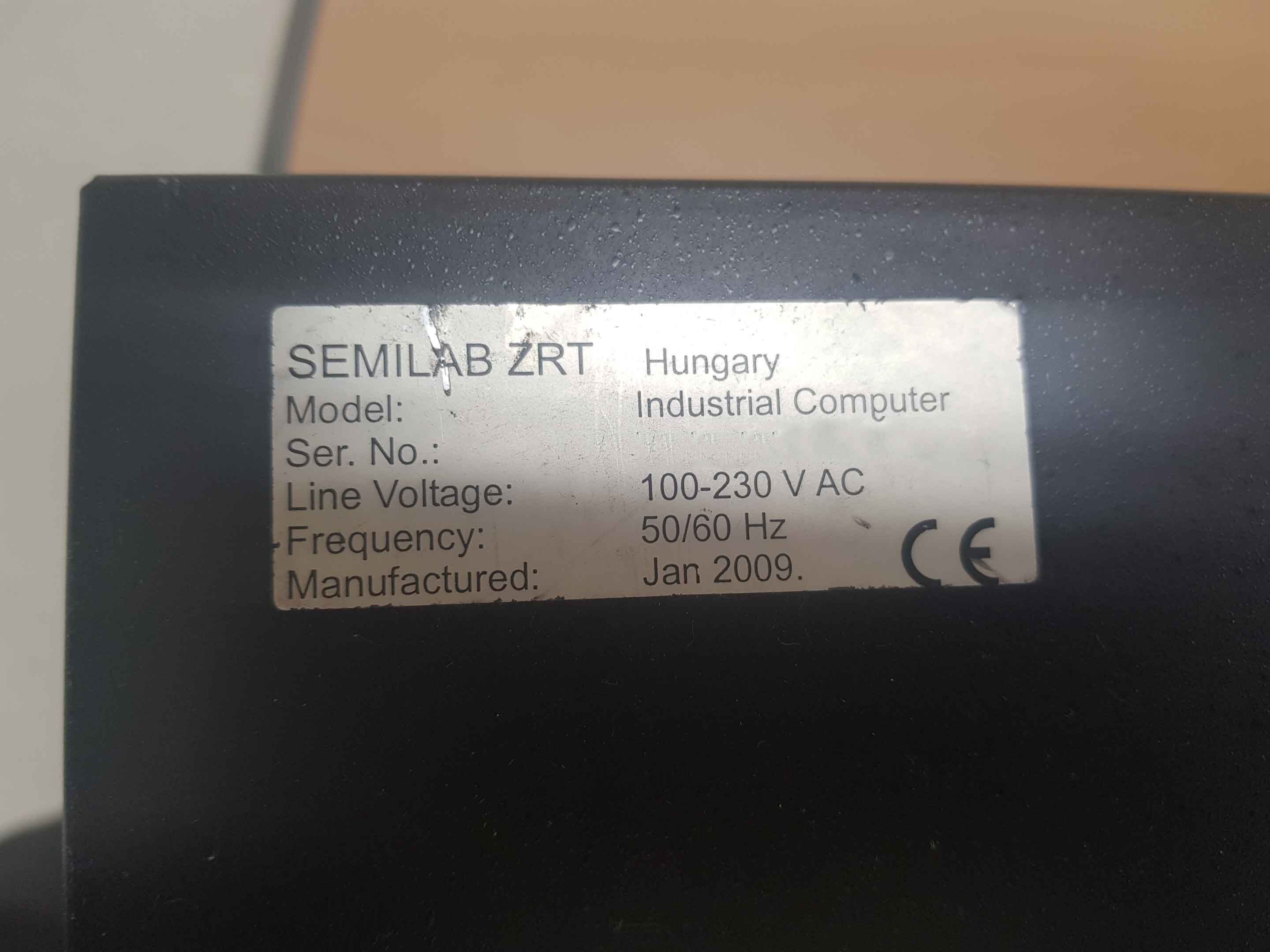



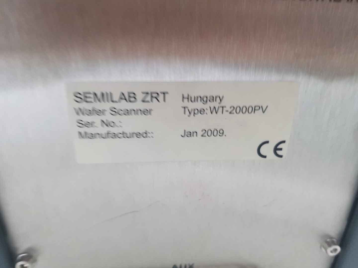


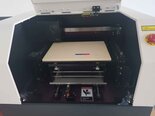
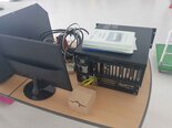
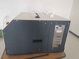
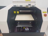
SEMILAB / SDI WT-2000PVN is a mask and wafer inspection equipment designed for semiconductor manufacturing. It is capable of scanning and inspecting a wide variety of mask, photomask, microlithography, and wafers up to 200mm. The system is also highly reliable and accurate as it can detect very small defects that are typically undetectable to the human eye. SDI WT-2000PVN is equipped with advanced lighting systems and a microscope with a long working distance. This allows the operator to quickly and accurately inspect the surface of a wafer without the need to move the wafer. The unit also features automatic focus and calibration control which enables high resolution imaging and greatly improves accuracy. SEMILAB WT-2000 PVN is capable of scanning and inspecting a wide variety of mask, photomask, microlithography, and wafers up to 200mm in size. It includes a built-in laser module with a scanning wavelength of 633nm, high-quality optics, and fast scanning speed of 5μm to enable inspection of large areas. The machine is also capable of autofocusing, so even if the surface of the wafer is uneven or curved, the image quality will remain sharp and clear. In addition, the tool is equipped with a built-in high quality inspection module for spotting microscopic defects such as particles, scratches, or cracks. This module can detect even the smallest defects on the surface of a wafer, enabling the operator to carry out in-depth analysis and take preventive action. SDI WT-2000 PVN is designed with an easy-to-use interfacing software which allows operators to easily monitor the scan process in real-time. The software also provides on-screen guidance and various image processing functions such as image averaging, image stitching, and image mask to ensure highest accuracy in detecting defects. Overall, SEMILAB / SDI WT-2000 PVN offers a high level of accuracy, speed, and reliability when it comes to the detection and analysis of microscopic defects on the mask and wafer surface. Its advanced optics and imaging systems ensure clear and sharp images every time, while its automated focus and calibration control allows operators to inspect large areas quickly and accurately. The user-friendly interface and built-in inspection module further enhance the overall accessibility and operating experience, making WT-2000PVN an ideal choice for any semiconductor manufacturing process.
There are no reviews yet
