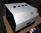
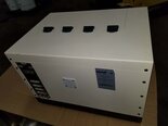
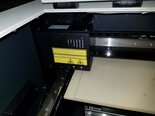
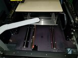
Used SEMILAB WT-2000 #9299523 for sale
URL successfully copied!
Tap to zoom


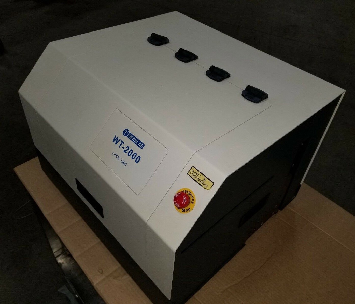

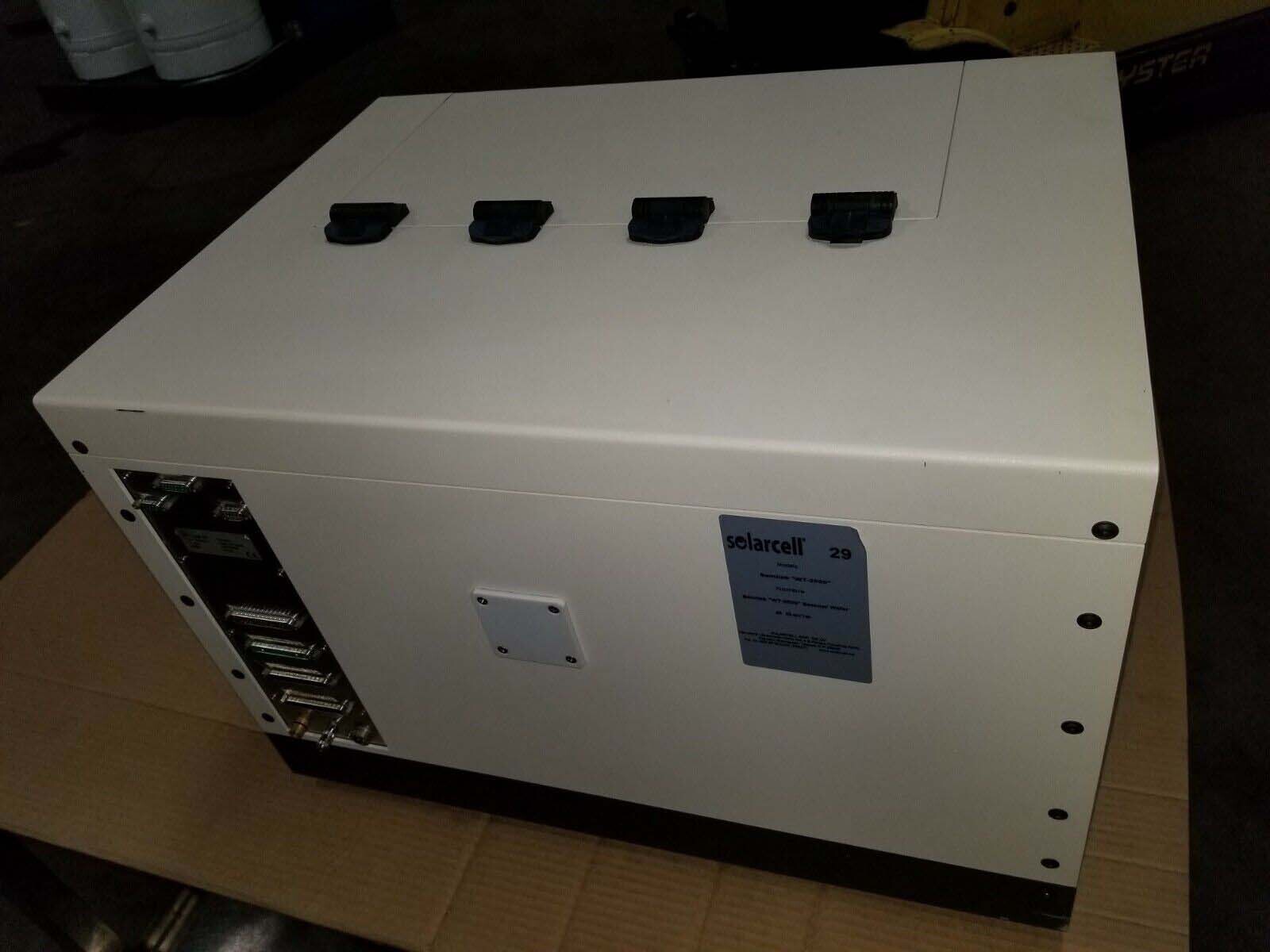


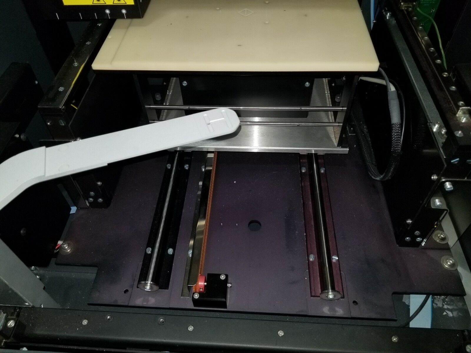

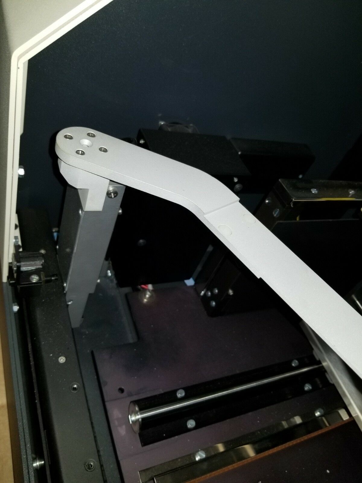


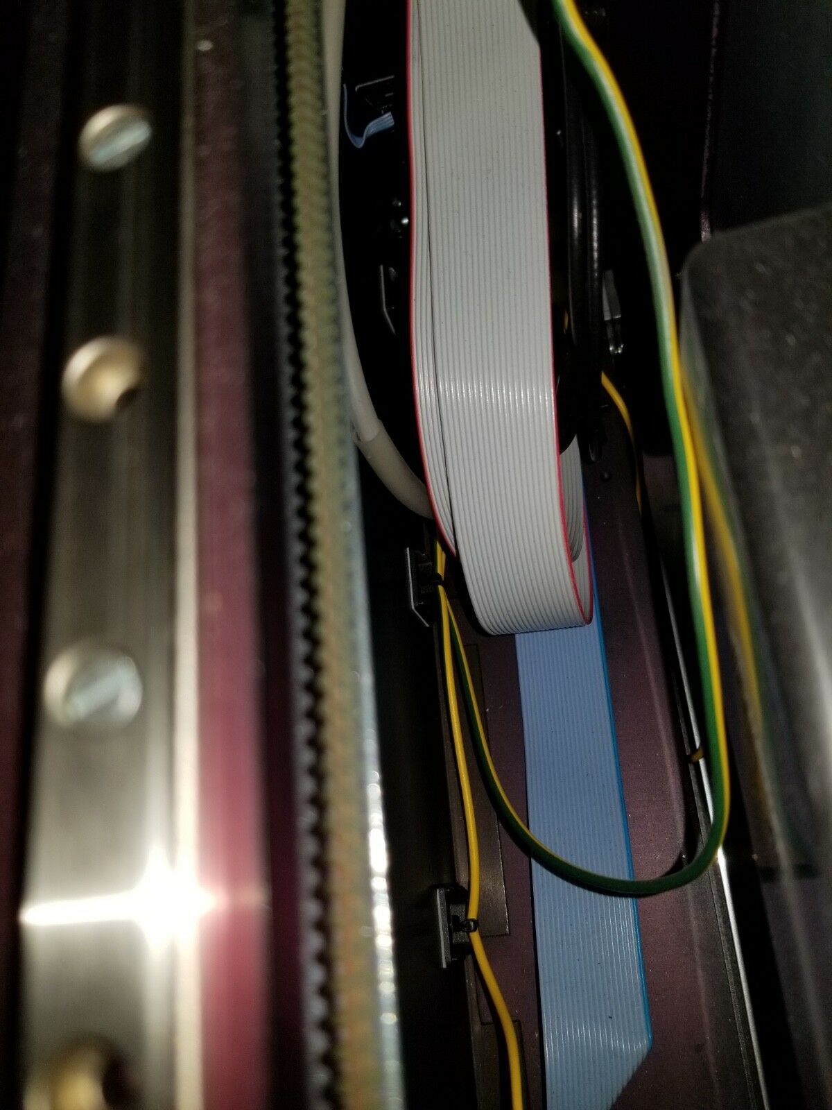

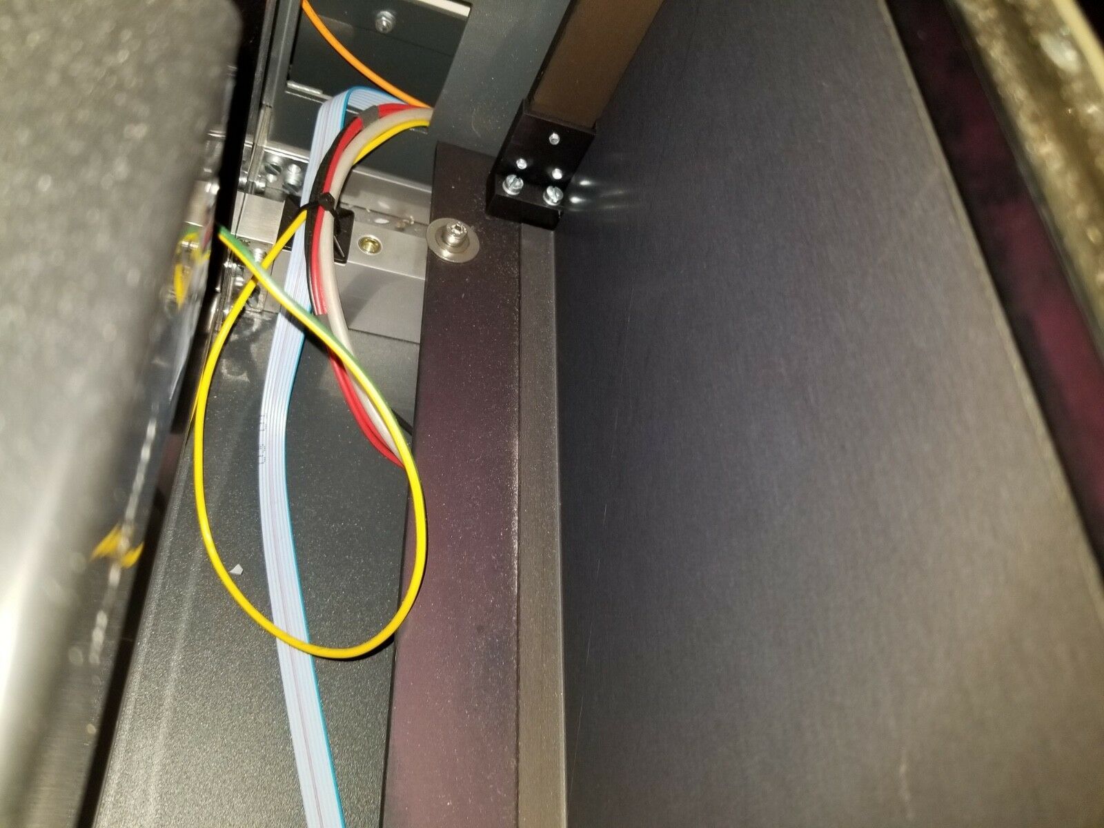


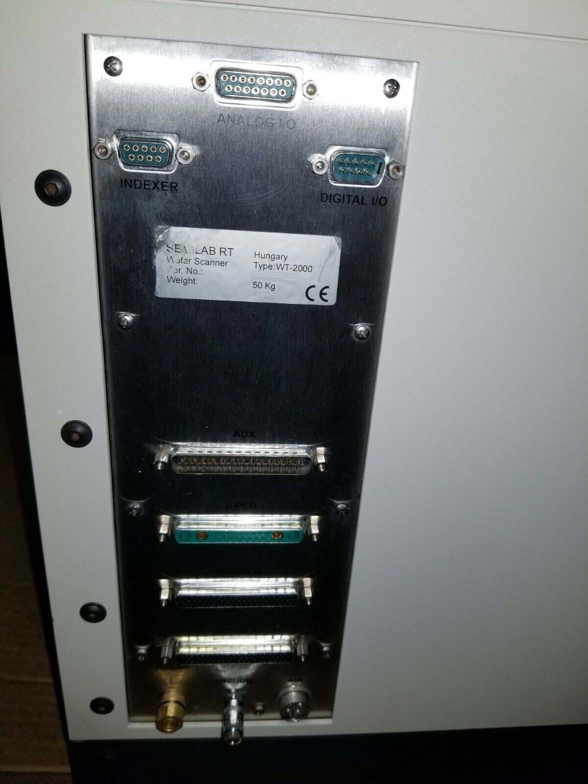

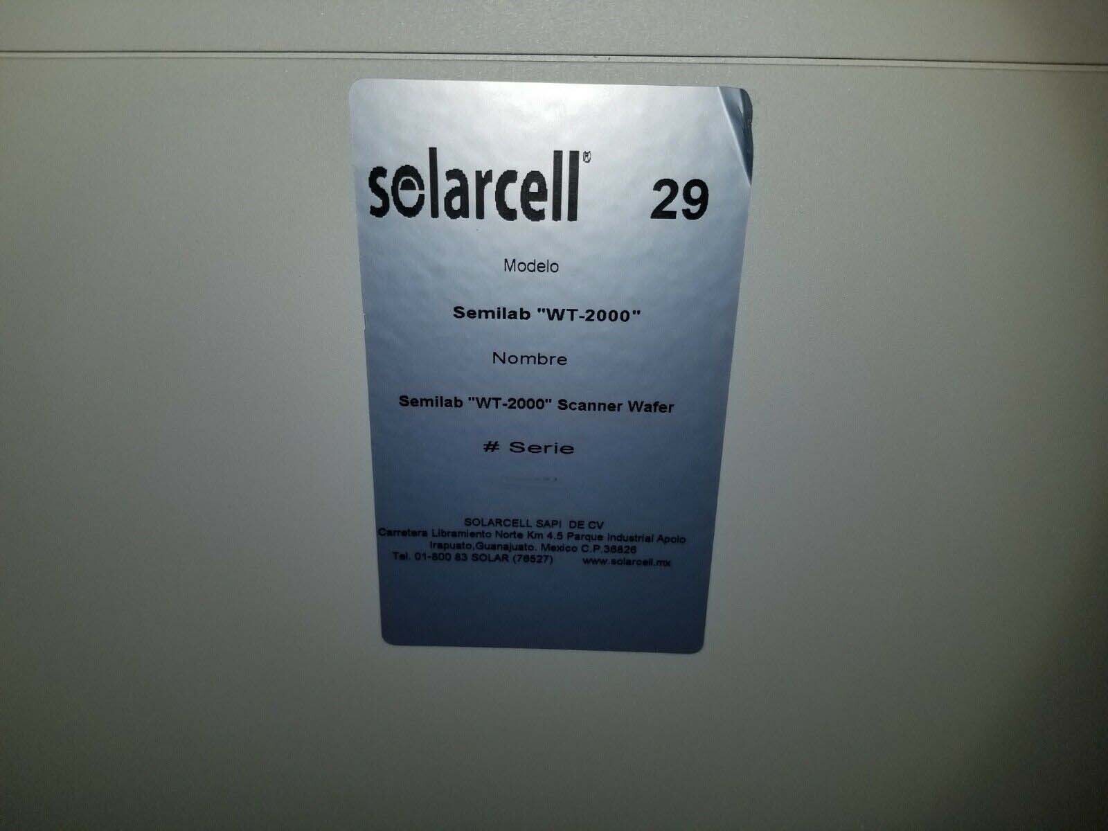

ID: 9299523
Vintage: 2010
Measurement system
µ-PCD LBIC
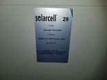
Solarcell 29
Does not include PC
2010 vintage.
SEMILAB WT-2000 is a high-precision mask and wafer inspection equipment designed to perform automated, non-contact, high-resolution measurements of topographies of flat surfaces. It is based on the acoustic imaging vibrometry (AIV) measurement technique, which measures the vibrations and responses of objects to a sound pulse. The system is able to measure dimensions with resolution below 0.5nm and is capable of achieving full area contactless measurements at high speed. SEMILAB WT2000 unit includes two main components: an acoustic imaging vibrometry (AIV) measurement head and a high resolution imaging machine. The AIV measurement head is responsible for generating acoustic pulses, receiving the reflected signals, and processing them into digital signals. The tool is capable of acquiring high-resolution topography data with axial resolution better than 0.5nm in the measuring range up to 2µm. The AIV measurement head's temporal resolution is set in the range of 125 to 500 ns. The imaging asset consists of a 522 nm visible laser, powered by a fiber-optic coupling emanating from the AIV measurement head. This laser-illuminated image is magnified by a high-resolution digital imaging model and collected by a digital camera. The high-resolution imaging equipment is based on a CCD camera with a pixel size of 3.45 μm and provides magnified images of up to 250 times. WT 2000 control system is responsible for controlling the apertures of the AIV measurement head for optimization of the measurement area, synchronization of the laser beam trigger for the imaging unit, and more. The user-friendly interface provides easy access to the machine functions for efficient and reliable operation and includes several standard features such as an automatic mask alignment procedure, a user-friendly navigation menu, and even a software feature for storing measurement parameters. In addition to the basic tool, SEMILAB WT 2000 offers an array of accessories for wafer and mask inspection. These accessories include special scanning quartz probes for surface roughness and topography profiling, a charger module for charging the sample for use in wet tension analysis, a microscope camera for visualization of small objects, an optical microscope for viewing small structures, and an eddy current sensor for measuring electrical conductivity. In conclusion, WT2000 is a powerful, high-precision mask and wafer inspection asset offering excellent repeatability and accuracy. Its hybrid approach combining acoustic imaging vibrometry and a high-resolution imaging model enables quick and easy measurement of topography, dimensions, roughness, and electrical properties of flat surfaces with high-resolution and speed.
There are no reviews yet
