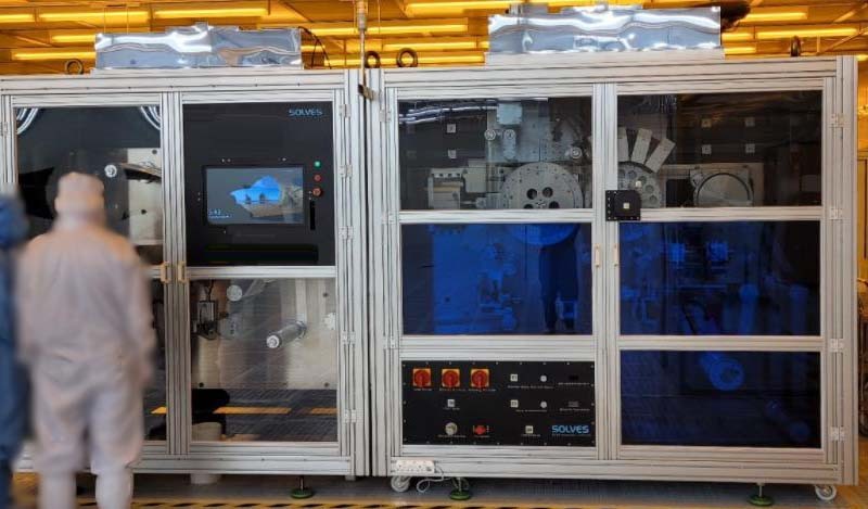
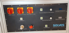
Used SOLVES NIL-157045-A #293590534 for sale
URL successfully copied!
Tap to zoom


ID: 293590534
Nano Imprint Lithography (NIL) system
Roll-to-roll
Thermal temperature: 200°C
Imprint spread: 3-30m/min
Throughput: Up to 20 meter/min.
SOLVES NIL-157045-A is an automated mask & wafer inspection equipment designed to quickly detect defects on masks and flat surfaces of wafers. It uses real-time image-acquisition, image analysis and 3D analysis technologies to detect both macro and micro defects at high resolution. The system features an integrated, full-screen viewing station featuring an advanced touch screen monitor and user interface to enable operators to easily locate defects for review and further characterization. The unit also has an automated 3D scanner that provides fast, automated measurements and defect assessment without the need for manual focusing or manual orienting. The state-of-the-art imaging machine uses a high-resolution line scan camera, an ultra-high sensitivity light source, and a highly accurate linear stage to create a high-definition image of each mask and wafer. The images are processed, filtered and then subjected to sophisticated computer-aided inspection and measurement (CAI) algorithms to detect subtle defects, even at very low resolutions. The tool also includes advanced error correction to reduce false alarms, as well as property control and defect rejection processes to prevent rejected defects from entering the manufacturing process. This helps ensure product quality and reliability while reducing the need for waste, reworking, and scrap. The asset is also equipped with an array of advanced tools and inspection algorithms, as well as a defect classification library, to further enhance defect review and characterization. These tools provide detailed information about each defect and enable fast and accurate correction or classification. This helps ensure quality of product, reduce manufacturing costs and maximize product yields. NIL-157045-A is a powerful model designed to provide rapid and reliable detection of defects on masks and wafer surfaces while reducing manufacturing costs. The equipment enables faster detection, more accurate defect identification and characterizations, more efficient defect research and correction, and improved product yields.
There are no reviews yet

