Used SOLVISION Precis 3D #293778479 for sale
URL successfully copied!
Tap to zoom
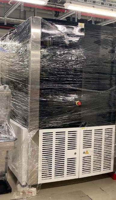

SOLVISION Precis 3D is a cutting-edge mask and wafer inspection equipment designed for advanced semiconductor manufacturing processes. This innovative tool incorporates state-of-the-art technologies to provide high-precision inspection capabilities for critical process steps in semiconductor fabrication. At the heart of Precis 3D is its advanced 3D inspection capability, which enables the system to accurately analyze the topography and critical dimensions of masks and wafers with nanometer-scale resolution. This high level of precision is essential for ensuring the quality and performance of semiconductor devices, as even tiny defects or deviations in feature sizes can impact the device's functionality and yield. The unit utilizes a combination of advanced imaging techniques, such as confocal microscopy, interferometry, and phase-shifting interferometry, to capture detailed 3D images of the surfaces of masks and wafers. These images are then processed using sophisticated algorithms to extract critical information about feature sizes, shapes, and positions, as well as detect defects such as particles, scratches, and pattern deviations. One key advantage of SOLVISION Precis 3D is its ability to perform both mask and wafer inspection in a single machine, eliminating the need for multiple tools and reducing the overall inspection time and complexity. This integrated approach also ensures consistent inspection results across different process steps, enabling better process control and yield improvement. The tool is equipped with advanced automation capabilities, including recipe-based inspection setups, automatic defect classification, and real-time monitoring of inspection results. This automation not only streamlines the inspection process but also reduces the potential for human errors and variability, leading to more reliable and repeatable inspection results. In addition to its high precision and automation capabilities, Precis 3D offers advanced defect review and analysis features, such as defect marking, sizing, and classification tools. These tools enable semiconductor engineers to quickly identify and analyze defects, understand their root causes, and take corrective actions to improve process efficiency and yield. Furthermore, the asset is designed to be seamlessly integrated into existing semiconductor manufacturing workflows, with flexible connectivity options and compatibility with industry-standard data formats. This integration capability enables easy data sharing and analysis across different process steps and tools, facilitating a holistic approach to process optimization and yield enhancement. Overall, SOLVISION Precis 3D represents a state-of-the-art solution for mask and wafer inspection in semiconductor manufacturing, offering high precision, automation, and advanced defect analysis capabilities to support the development of next-generation semiconductor devices. By leveraging the model's cutting-edge technologies and capabilities, semiconductor manufacturers can achieve higher process yields, improved device performance, and greater competitiveness in the global semiconductor market.
There are no reviews yet