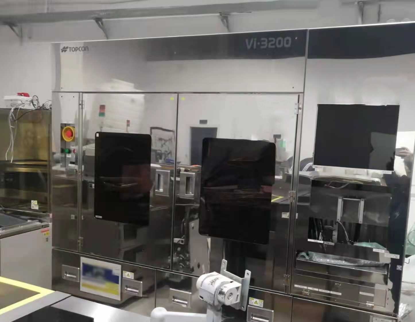
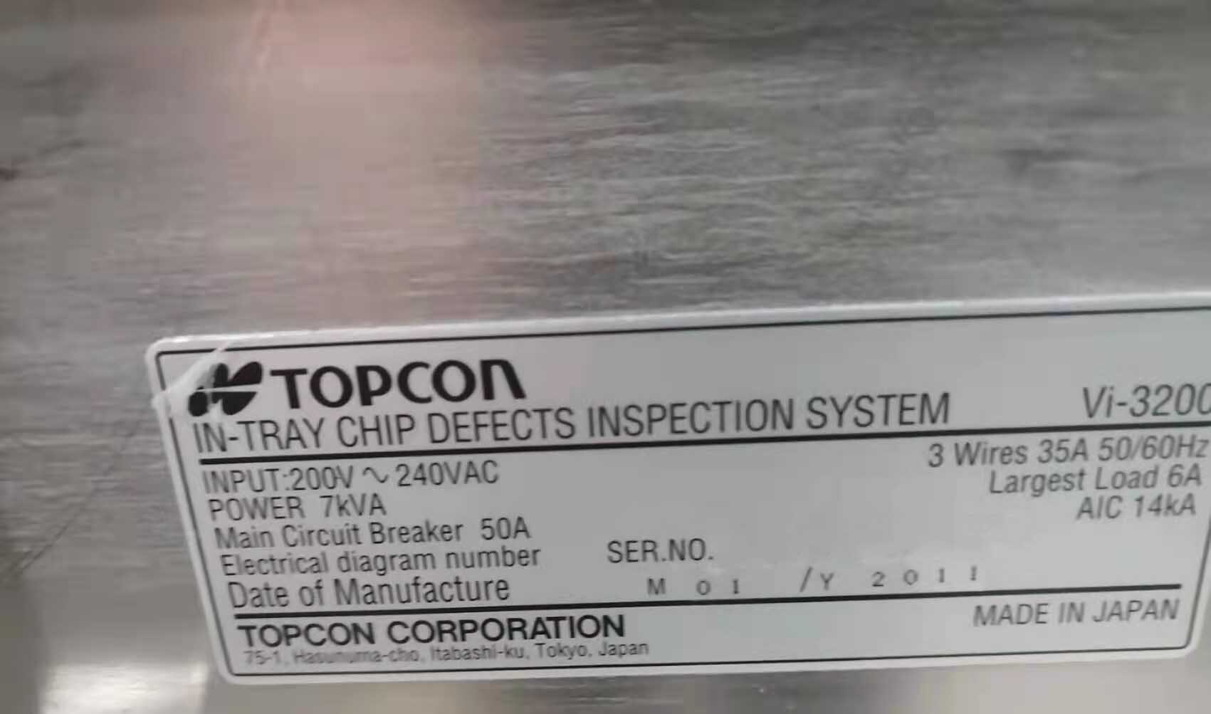
Used TOPCON VI-3200 #9410949 for sale
URL successfully copied!
Tap to zoom


TOPCON VI-3200 is a high-throughput mask and wafer inspection equipment designed for use in the semiconductor industry. It provides top-of-class imaging and automated defect inspection performance, helping to ensure optimum process control and cost savings. VI-3200 uses brightfield, darkfield, and Wafer Spectrum Imaging (WSI) to provide a comprehensive suite of inspection capabilities. Brightfield imaging is used to detect size and location-based defects, while darkfield imaging detects pattern irregularities and line width variations. WSI effectively captures the exact shape, position and condition of a wide range of defects, including voids, scratches and contamination specks. The system offers superior image detail and accuracy, as well as an impressive mix of capabilities including automated inspection setup and parameter optimization, 3D image analysis, and comprehensive defect analysis. Its automated inspection setup and parameter optimization features allow the unit to quickly optimize settings to the job at hand, while its 3D image analysis capabilities provide high-precision measurements of pattern and alignment errors. TOPCON VI-3200 has an advanced defect analysis capability that includes pattern recognition and quantitative analysis of aerial images, enabling the identification of small-sized levels. To ensure superior image quality and maximum performance, the machine is equipped with a next-generation optical tool, as well as a high-performance image processor. The asset is designed for quick, easy setup and operation, making it well-suited for busy production environments. It also features a wide range of integrated quality and defect measurement functions,including 2D/3D optical critical dimension measurements, which can be used to analyze and measure large, complex mask patterns. VI-3200 is a powerful, highly capable mask & wafer inspection model that combines superior image quality and accuracy with an impressive range of capabilities. By helping to ensure optimum process control and cost savings, it is an excellent choice for semiconductor fabrication environments.
There are no reviews yet

