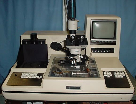
Used VIKING / DYMATIX VIS 100D #19172 for sale
URL successfully copied!
Tap to zoom


ID: 19172
Wafer Size: 6"
Wafer Inspection Station, 6" capacity with computer control Olympus trinoccular microscope, 50 & 100 x, video camera & digitizer, RS232
Computer is not Windows based.
VIKING / DYMATIX VIS 100D is a high-precision Mask & Wafer Inspection Equipment designed for the semiconductor industry. The system provides efficient and comprehensive defect detection for a variety of mask and wafer substrates. It features a wide range of inspection parameters and a high thermal drift compensation capability to ensure high throughput. VIKING VIS 100D provides a fully automated wafer pipeline with advanced optics and image processing technology. The unit utilizes an advanced linear array style beam scanning design which ensures high throughput, low positional drift and high-resolution imaging. This ensures a rapid and reliable inspection process. Additionally, the machine features an optimally tuned illumination source and advanced imaging optics, with superior control of diffraction and scatter while maintaining low aberrations. The tool supports multiple mask and wafer substrates, with shape and size variations, ensuring high flexibility and throughput. The asset offers enhanced defect detection capabilities, with its powerful image processing algorithms. These algorithms include global and local intensity comparisons, dilation, geometrical pattern matching, and full automated reporting of inspection results. DYMATIX VIS 100D includes an intuitive user interface, with easily accessible parameters to ensure simple and fast operation. Highlighted features include a unique low-noise detector, which is resistant to thermal drift and can attain high-sensitivity measurements, at extreme angles and angles of incidence. The model is also capable of providing a high dynamic range of 0.1µm to 50µm for a wide range of shapes, size, and pitch of detected defects. Its pixel cell structure also enables high-resolution visualization, up to 1.5nm. Moreover, its advanced image data management, image area correction, artifact removal and pattern generation capabilities ensure accurate and reliable defect detection. VIS 100D meets a variety of applications needs, featuring a number of features and components, including advanced optics and illumination systems, highly optimized detection and imaging systems, advanced image processing algorithms and high-resolution imaging. It is designed for use in complex semiconductor applications, providing efficient and reliable inspection capabilities for mask and wafer substrates.
There are no reviews yet