Used ZEISS AIMS Fab 193 Immersion #9221855 for sale
URL successfully copied!
Tap to zoom
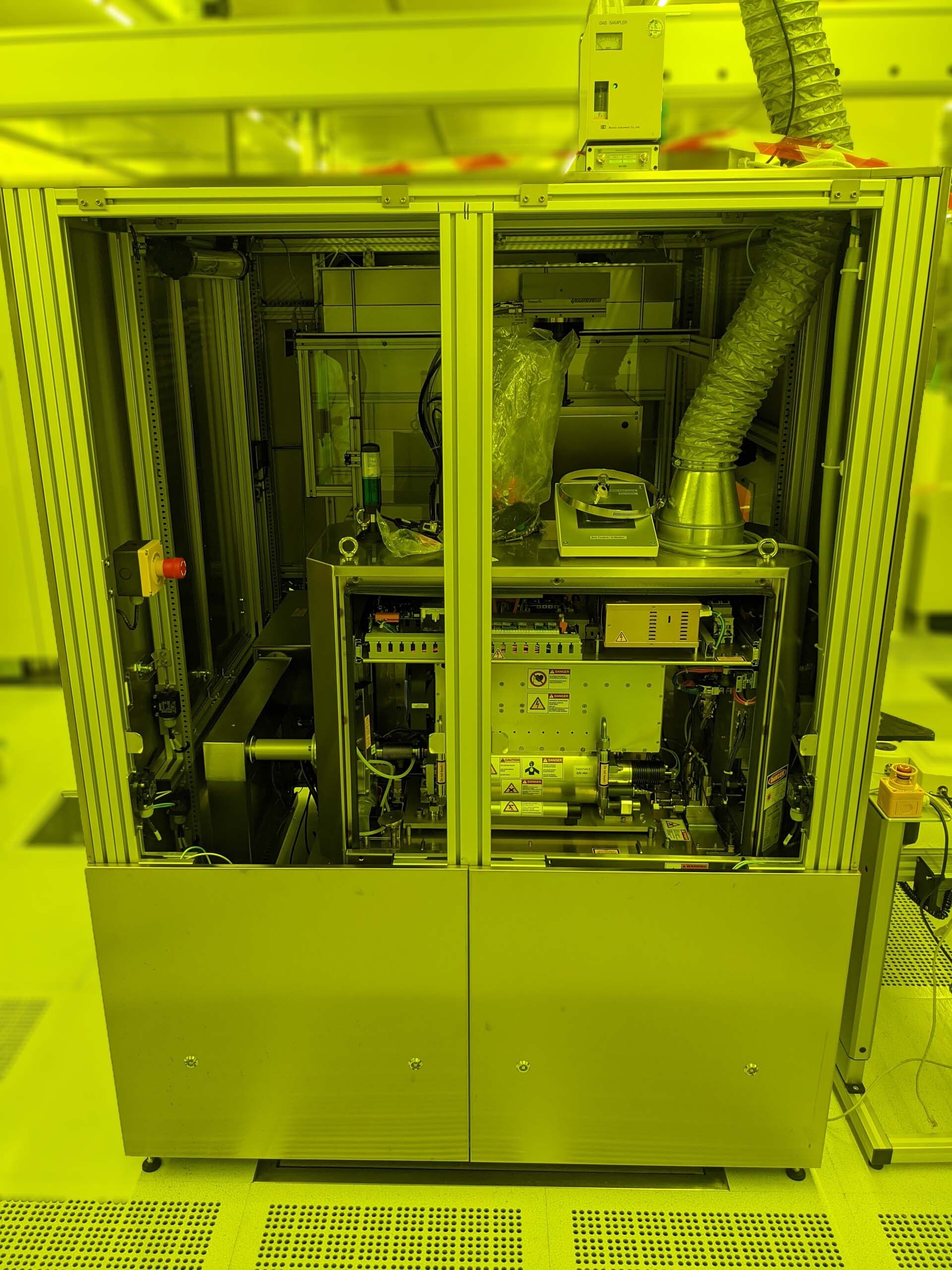

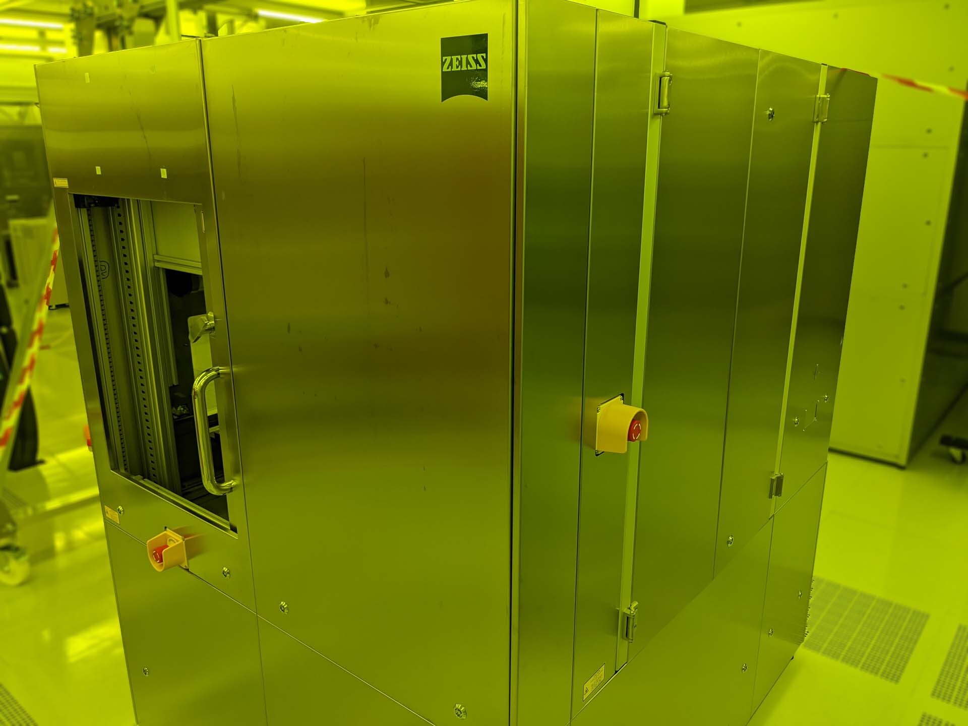

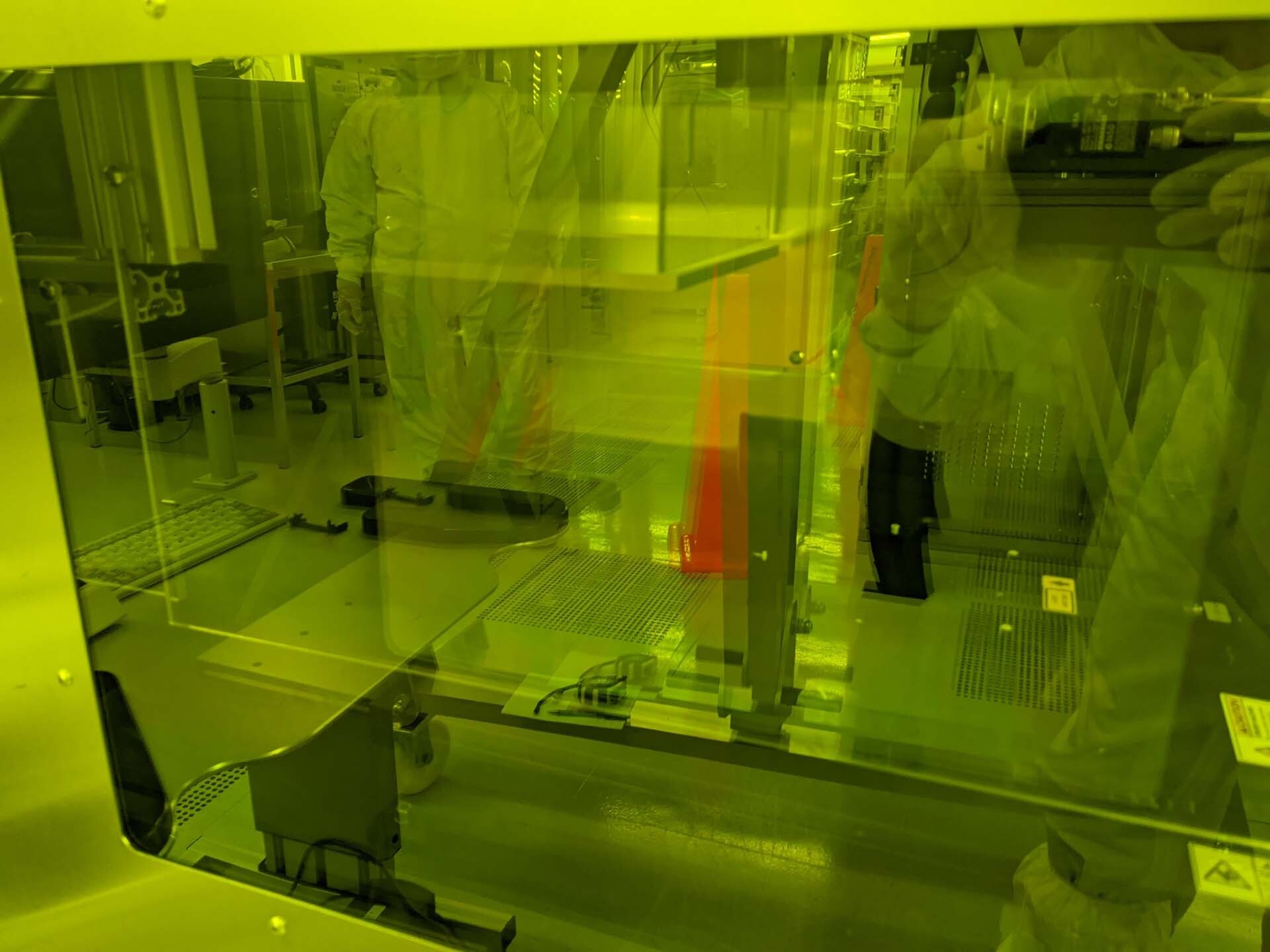

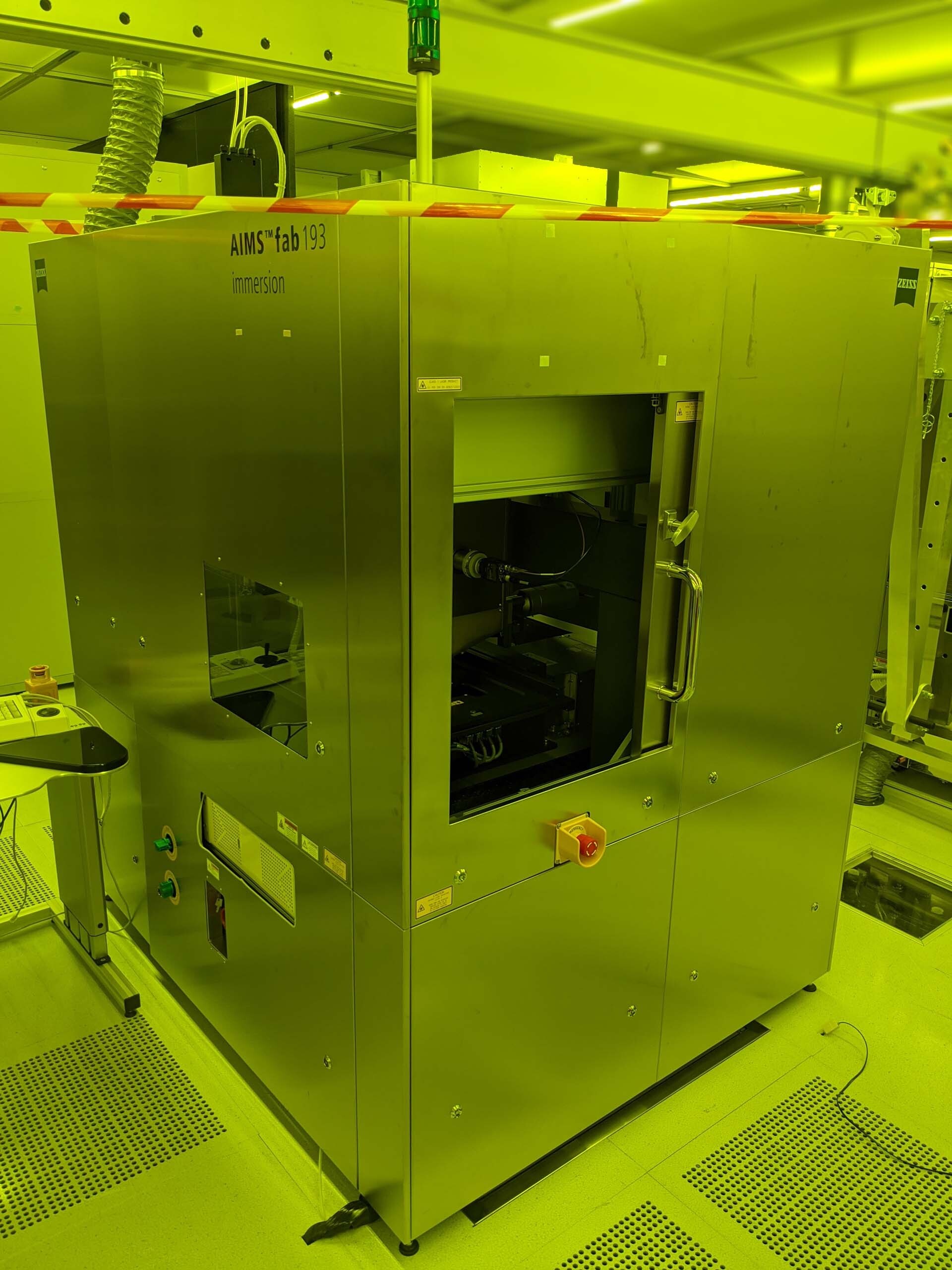

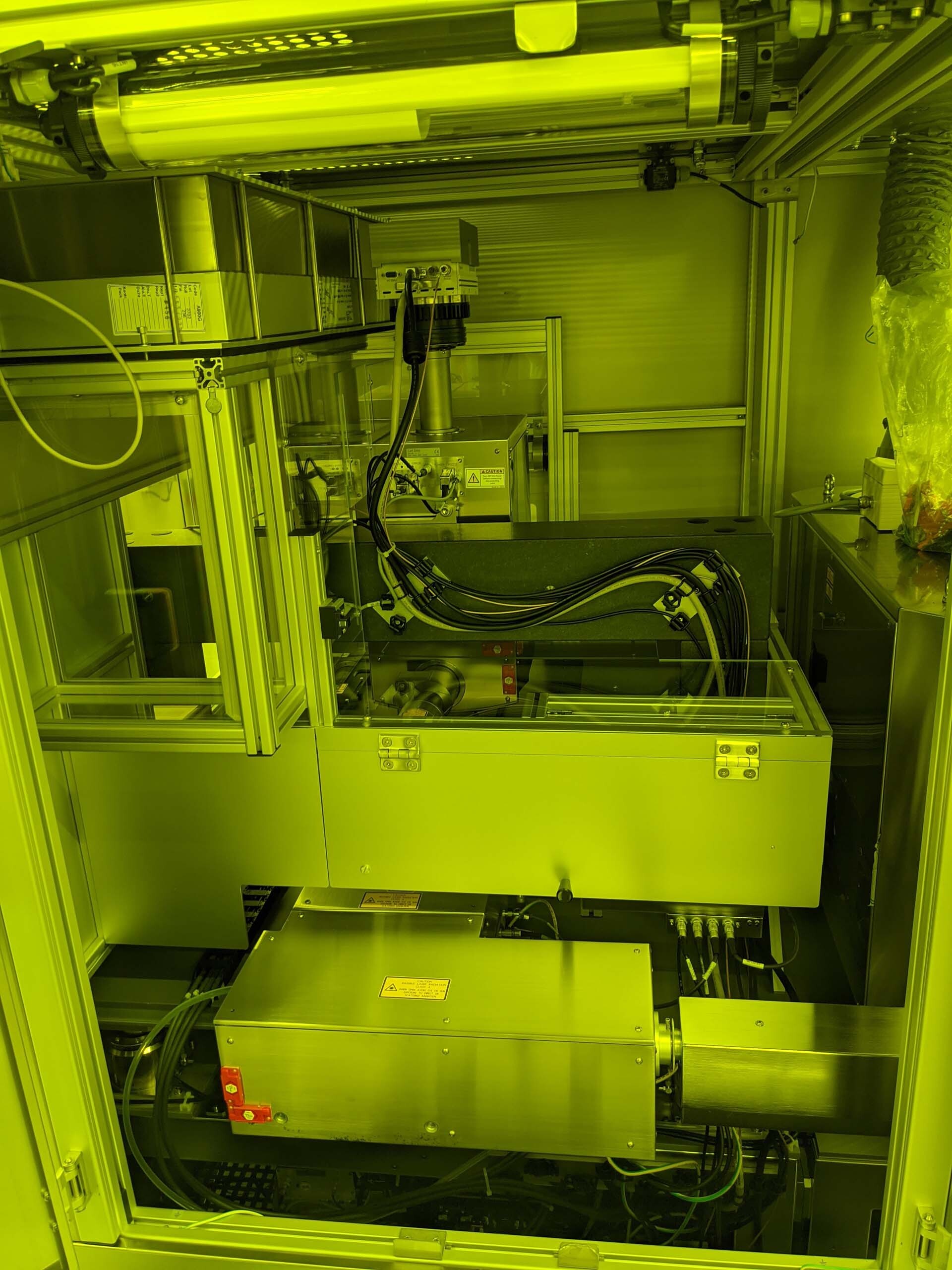

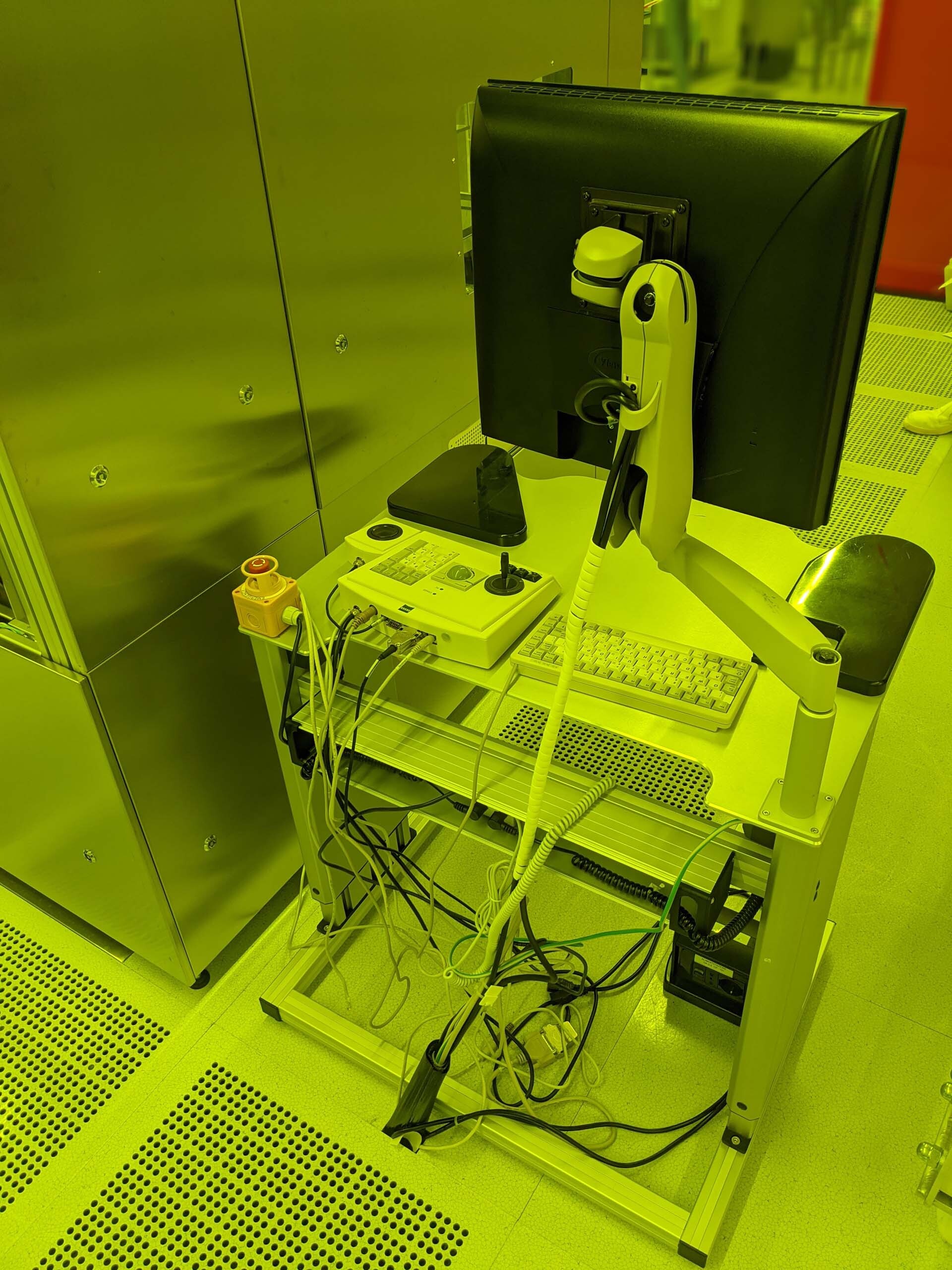

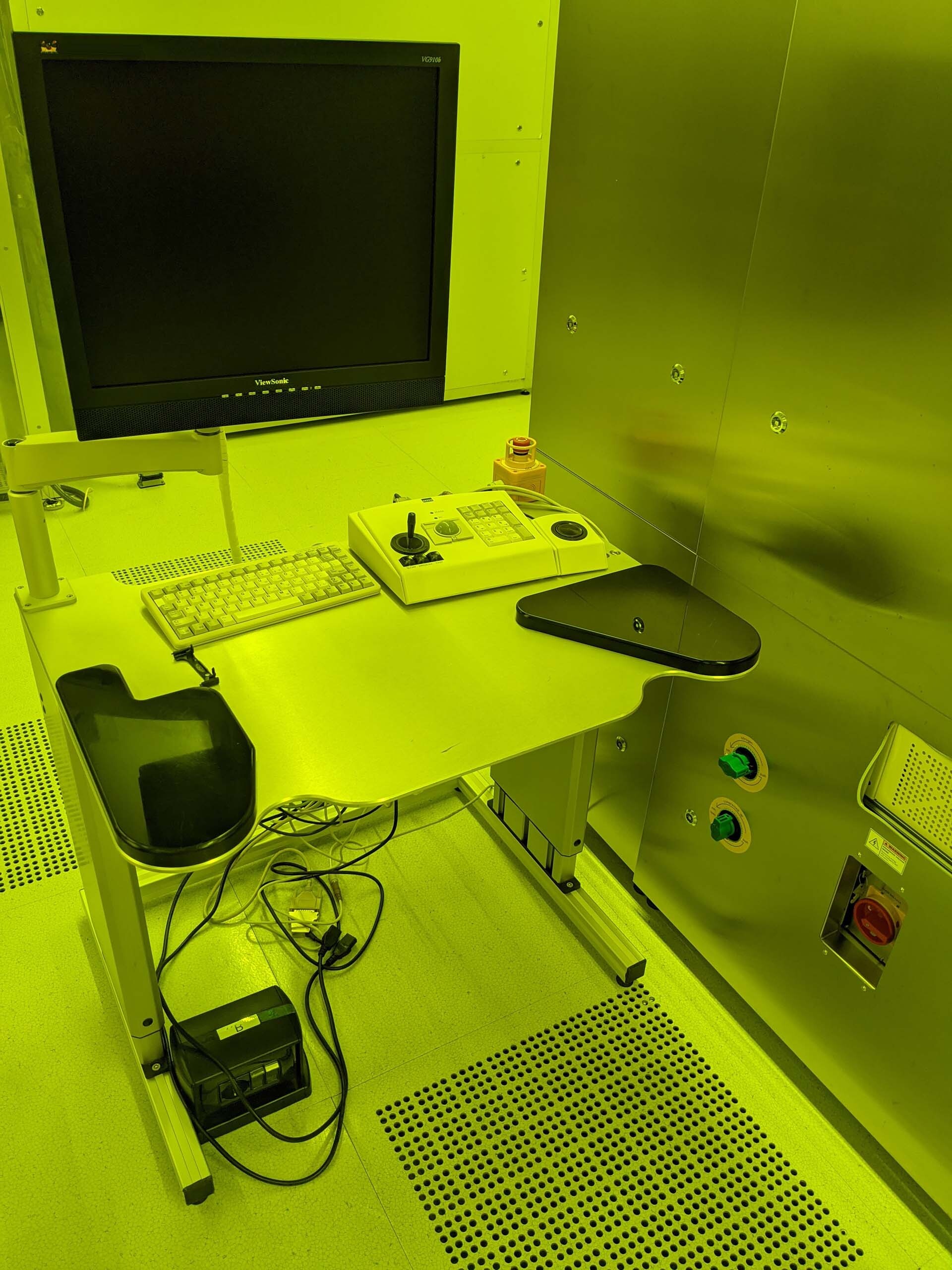


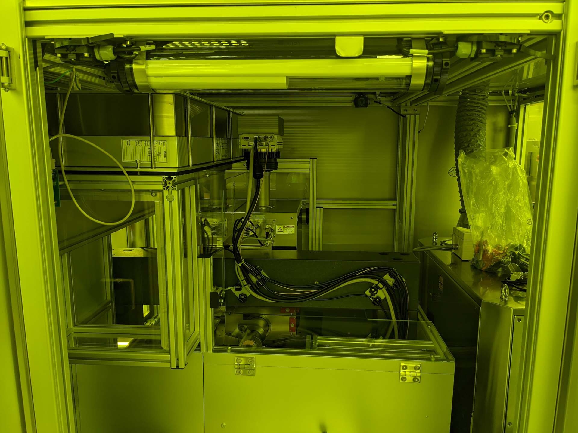

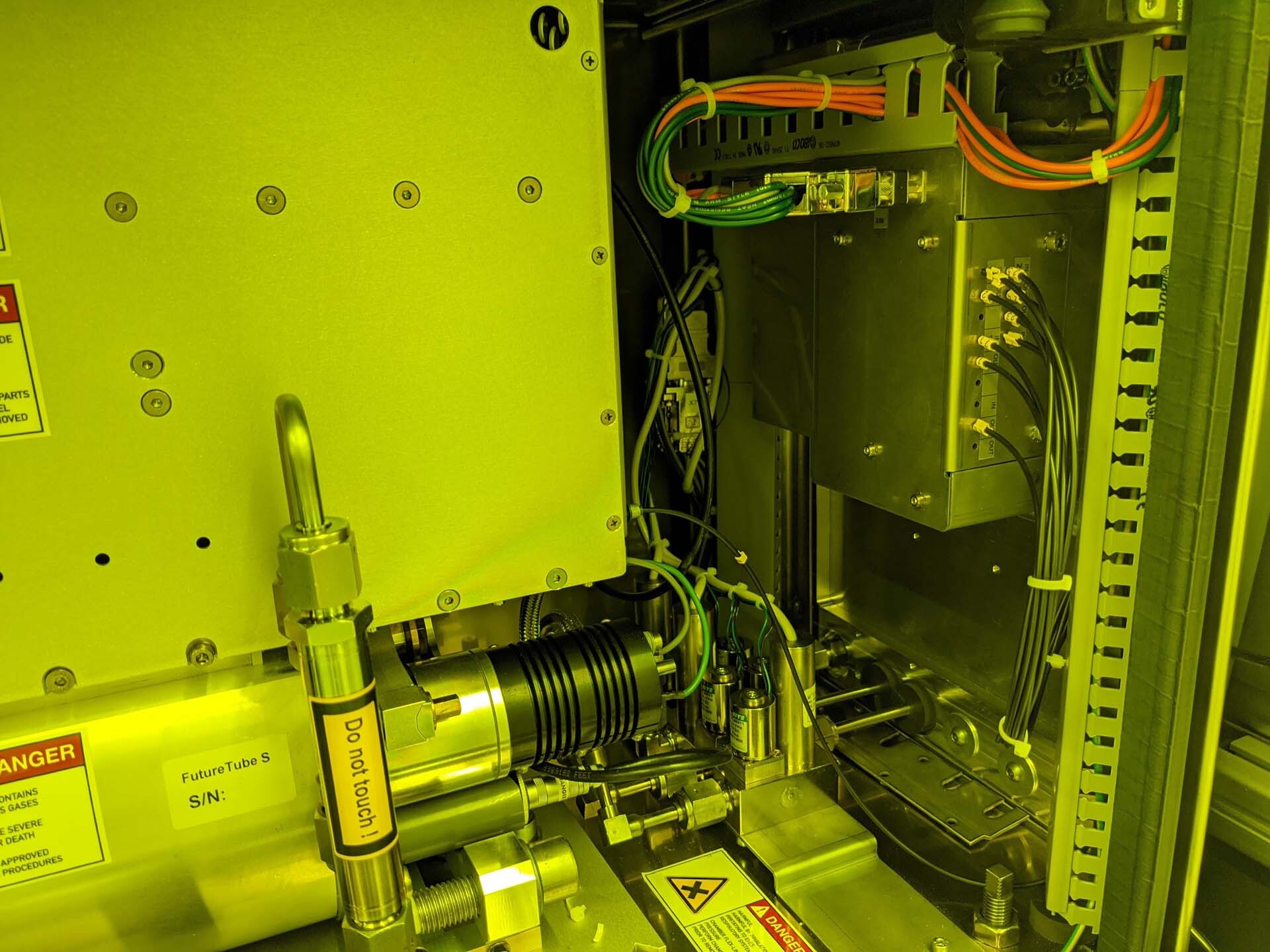


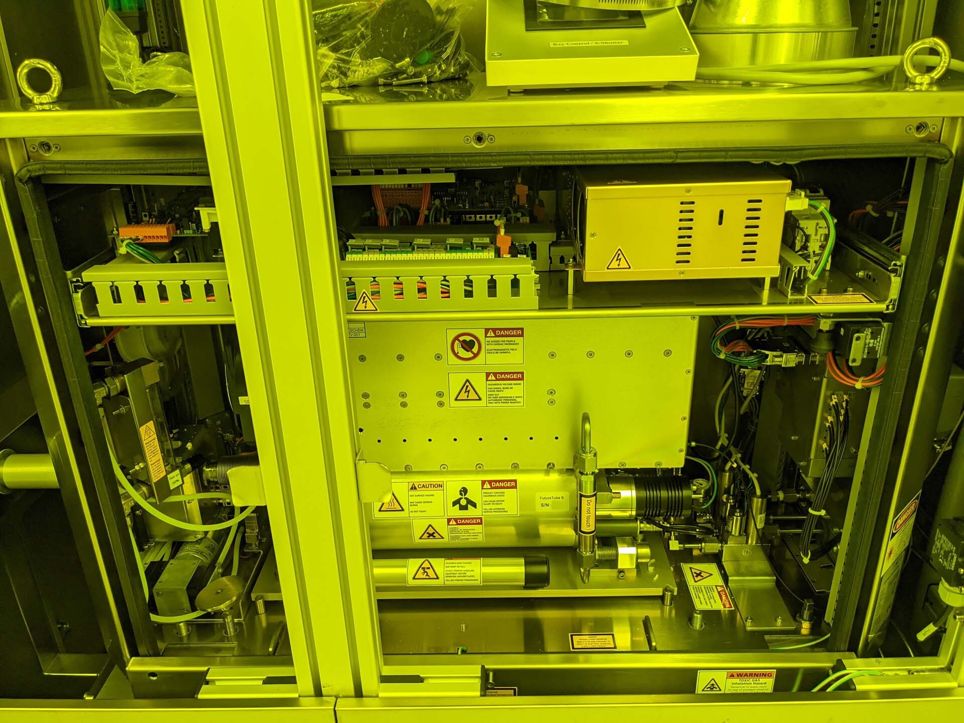

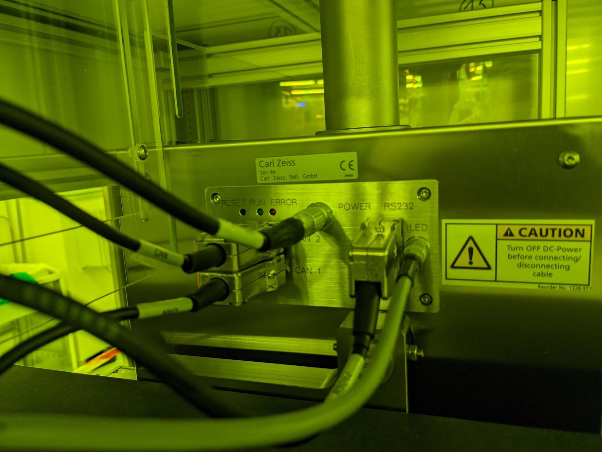

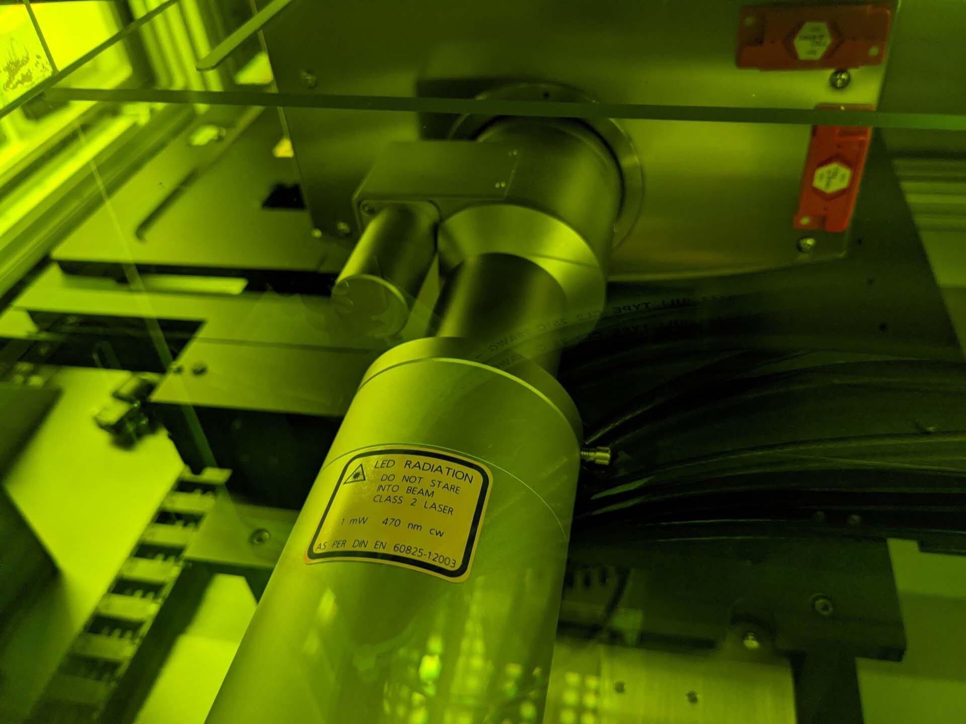

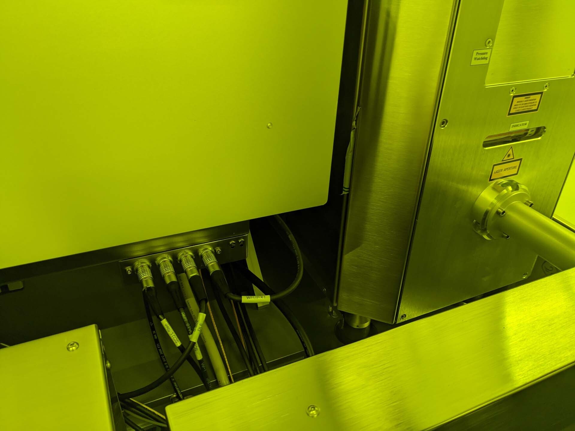









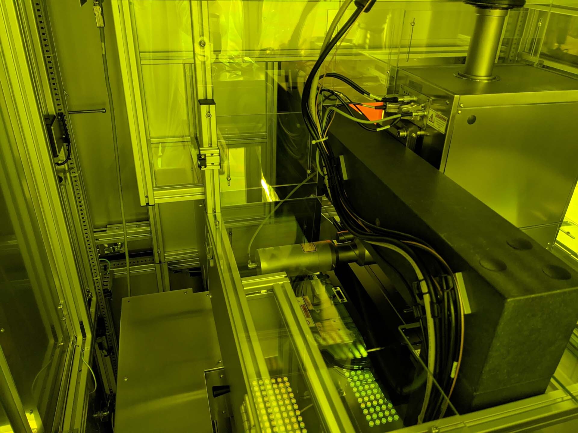

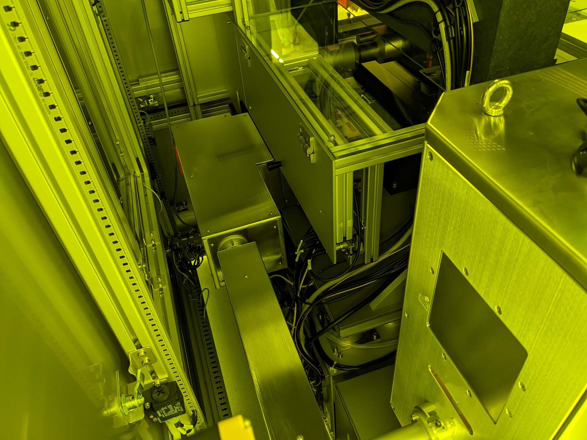


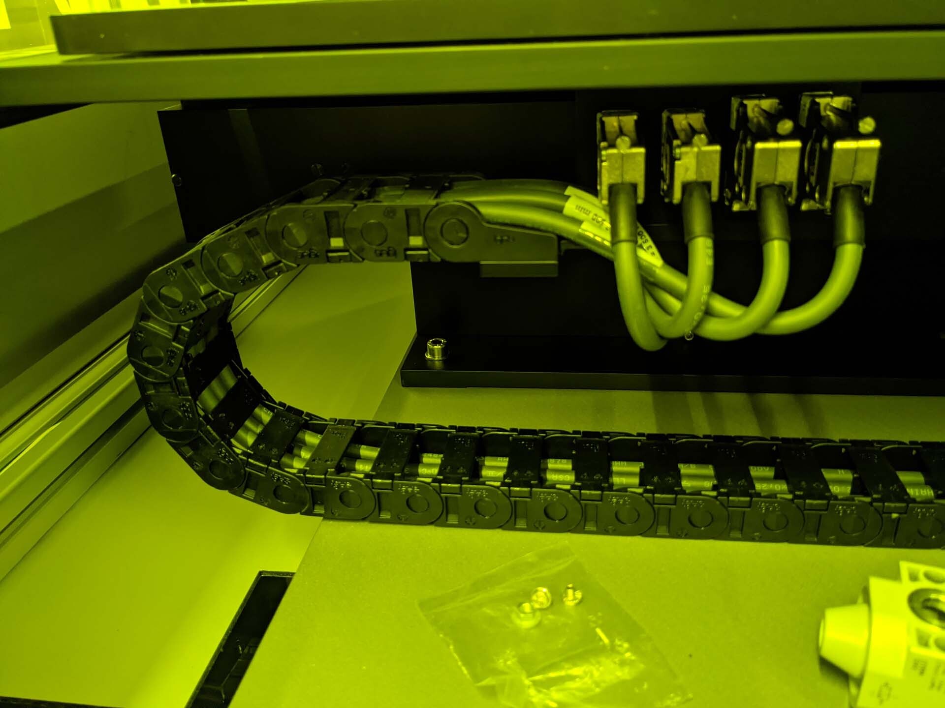

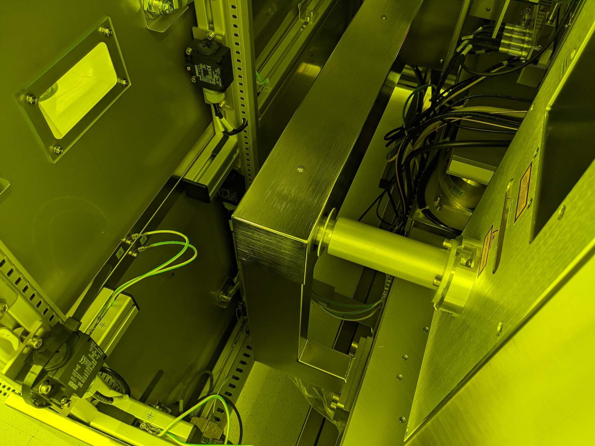





ID: 9221855
Wafer Size: 6"
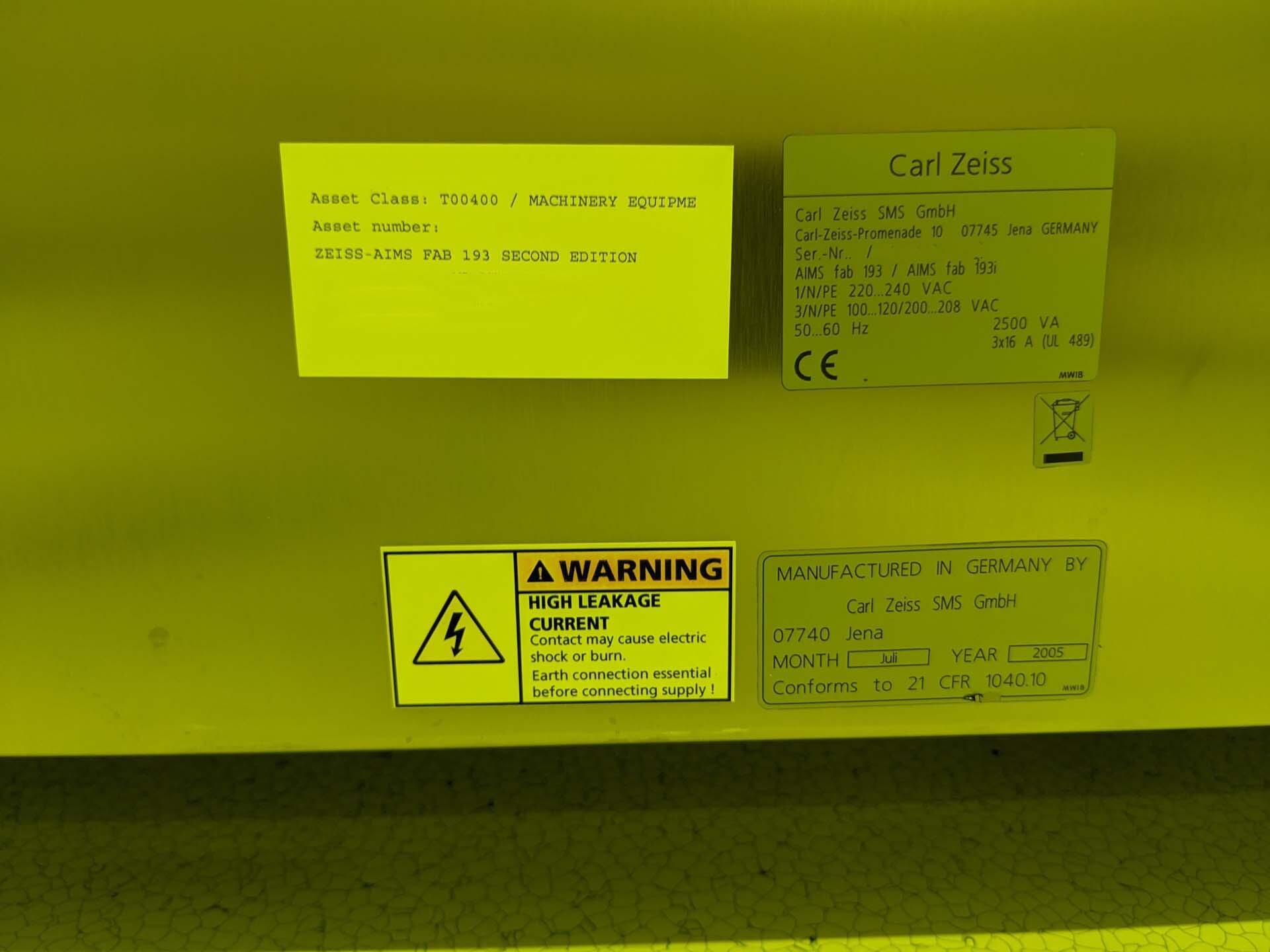
Vintage: 2005
System, 6"
Laser to be replaced
Laser gas manifold to be replaced
2005 vintage.
ZEISS AIMS Fab 193 Immersion is an advanced advanced mask and wafer inspection equipment. It uses a 193nm immersion ArF laser source and is capable of inspecting wafers up to 200mm in diameter, with a maximum wafer exposure of 16mm. Its advanced image processing algorithms enable rapid and accurate analysis of device performance in a wide range of materials and photomask defects. AIMS Fab 193 Immersion incorporates several features that make it unparalleled in the wafer inspection market. Its maximum 256 kV accelerating voltage enables highly accurate imaging of device features in nanometer resolutions. It is also capable of looking at dense line patterns with both up to 64X magnification and detailed pattern-based metrology. Additionally, its Depth Of Focus (DOF) technology allows wafers to be inspected through different depths within the same layer, enabling a deeper understanding of device structure. In addition to its advanced imaging capabilities, ZEISS AIMS Fab 193 Immersion also provides powerful process control features. Through its software interface, the user can control the system's process parameters such as exposure time, focus depth, and acceleration voltage. Furthermore, its in-unit 3D auto-focus algorithm allows the machine to focus on different target layers. By combining this auto-focus feature with its state-of-the-art image processing algorithms, AIMS Fab 193 Immersion quickly and accurately locates defects and abnormalities in products. Finally, ZEISS AIMS Fab 193 Immersion tool is designed with ease-of-use in mind. Its huge viewing screen enables an easy navigation of the user interface and greater visibility of the sample. Its touch screen control panel supports advanced features such as user-defined algorithms, pattern-matching and real-time imaging for quick and efficient inspection. Overall, AIMS Fab 193 Immersion asset offers unparalleled image resolution, advanced process control capabilities, and ease-of-use. Its features make it ideal for inspecting wafers and photomasks with high accuracy, while providing a comprehensive insight into device performance.
There are no reviews yet

