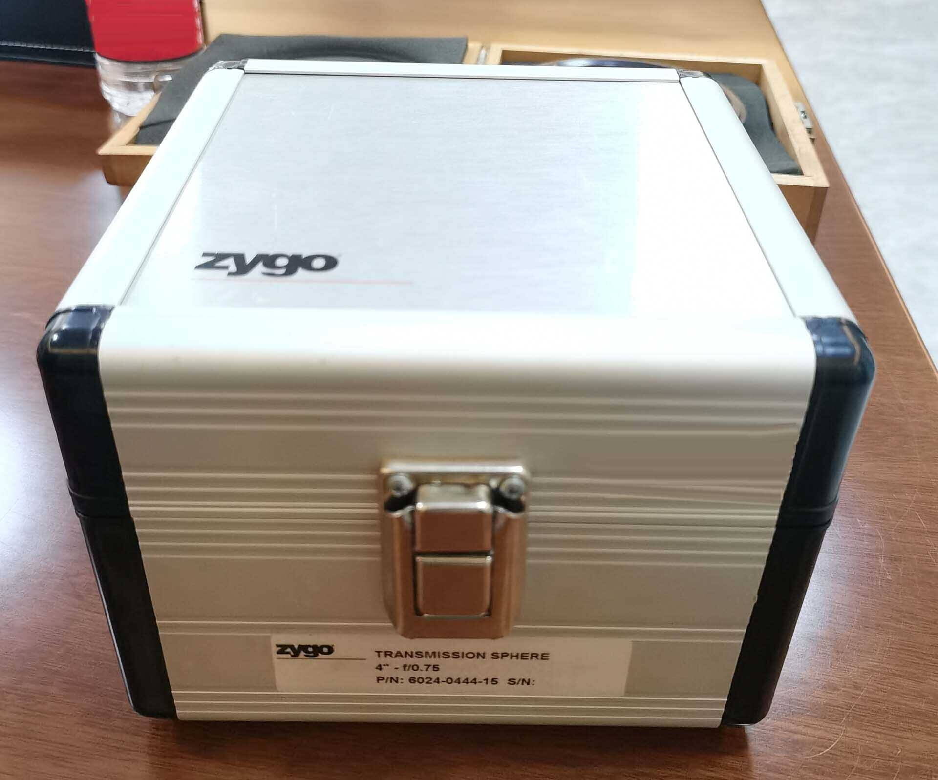
Used ZYGO F/0.75 Lambda/40 #9383775 for sale
It looks like this item has already been sold. Check similar products below or contact us and our experienced team will find it for you.
Tap to zoom


Sold
ZYGO F/0.75 Lambda/40 mask and wafer inspection equipment is a high-precision optical system designed to detect defects in photomasks and wafers used in semiconductor device manufacturing. The unit is capable of inspecting surfaces down to a resolution of 0.75 microns, and offers advanced features such as automatic focus tracking and full-field image stitching. At the core of the machine is a large-format laser-based illumination source which produces light with a wavelength of 40 nanometers. This allows for the inspection of even the smallest features of the photomask or wafer before it is passed to the next step in the production process. The illumination source is accompanied by a pair of advanced cameras which enable the detection of defects in a variety of formats, including color, brightness, and contrast. The cameras are mounted onto a movable platform which allows for easy placement of the cameras at any area on the photomask or wafer. The tool also includes an integrated vision processor which can combine multiple images from the two cameras to create a single image of the entire area for inspection. This processor is also used to detect defects in the image and store the data for later review. ZYGO F/0.75 Lambda/40 mask and wafer inspection asset is equipped with a range of features to make the inspection process faster and more efficient. It has a large working area, allowing for inspection of a larger wafer in one scan. The automatic focus tracking feature ensures that the inspection process is as accurate and precise as possible. Additionally, the model comes with software which enables the user to customize the processing parameters and set up consistency checks to ensure that no defects are overlooked. ZYGO F/0.75 Lambda/40 mask and wafer inspection equipment delivers reliable results for defect analysis, allowing users to ensure that their products meet the highest standards of quality. This system is suitable for use in both high-volume and low-volume production runs, making it an ideal tool for the semiconductor industry.
There are no reviews yet