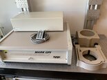
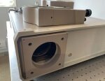
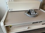
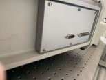
Used ZYGO Mark GPI-XPS #9258818 for sale
URL successfully copied!
Tap to zoom









ID: 9258818
Interferometers
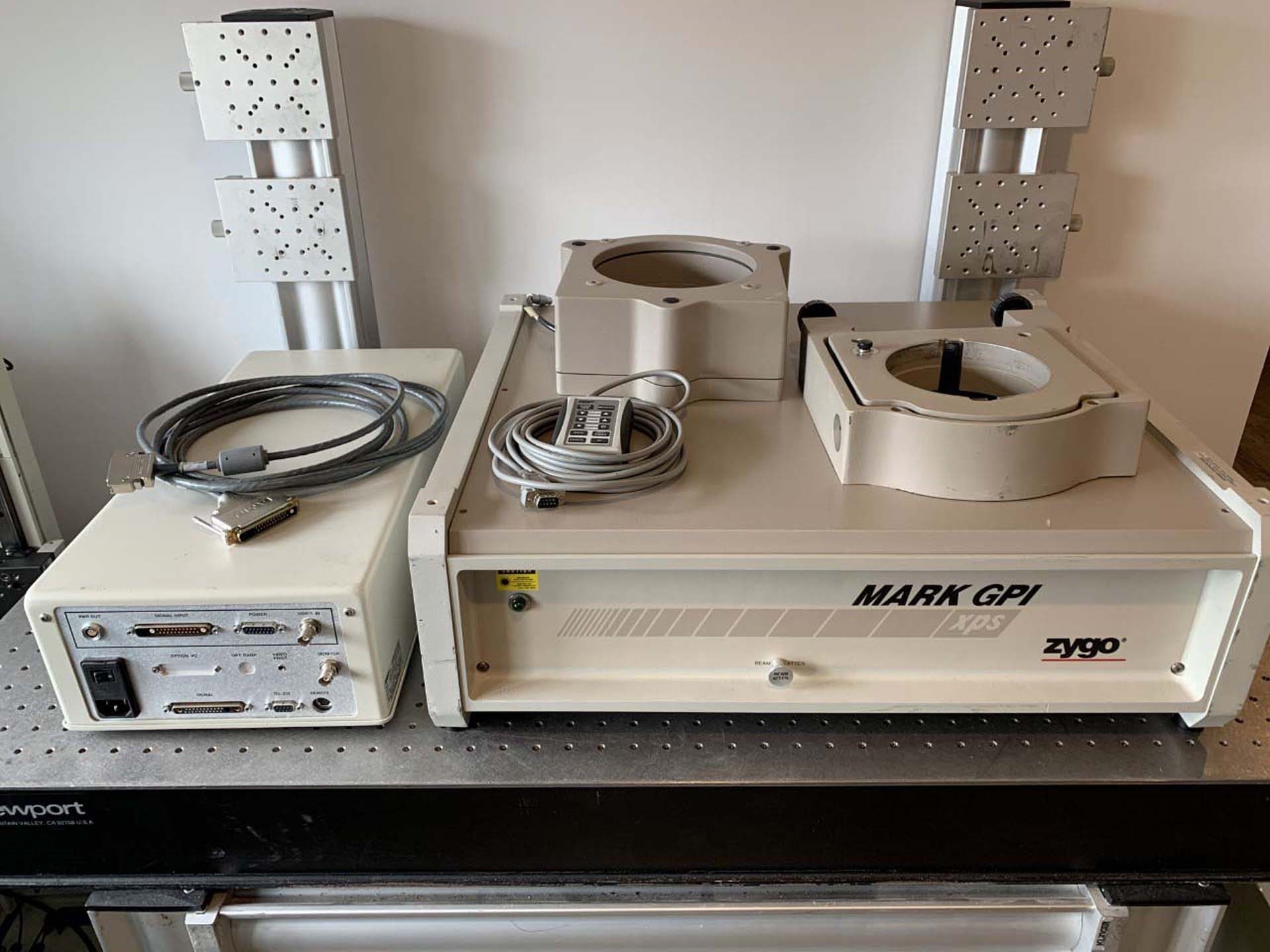
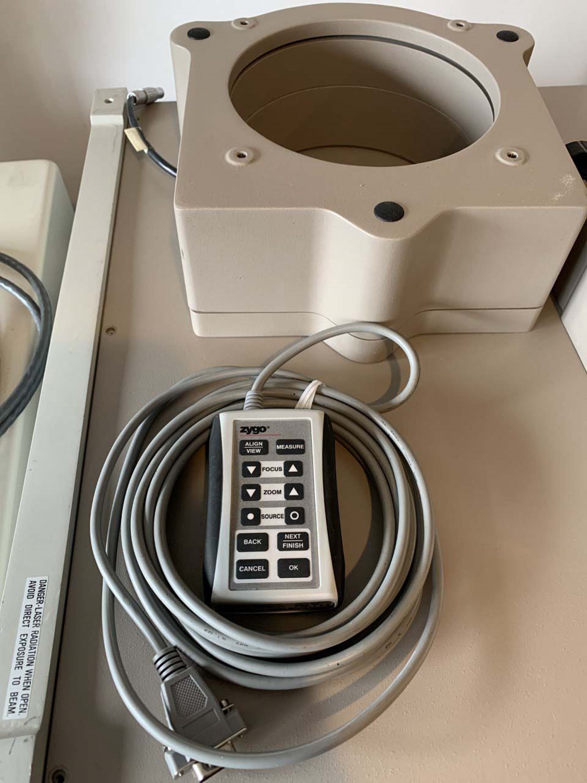
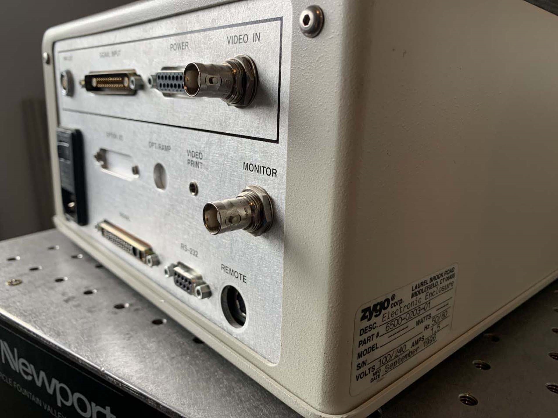
GPI Controller
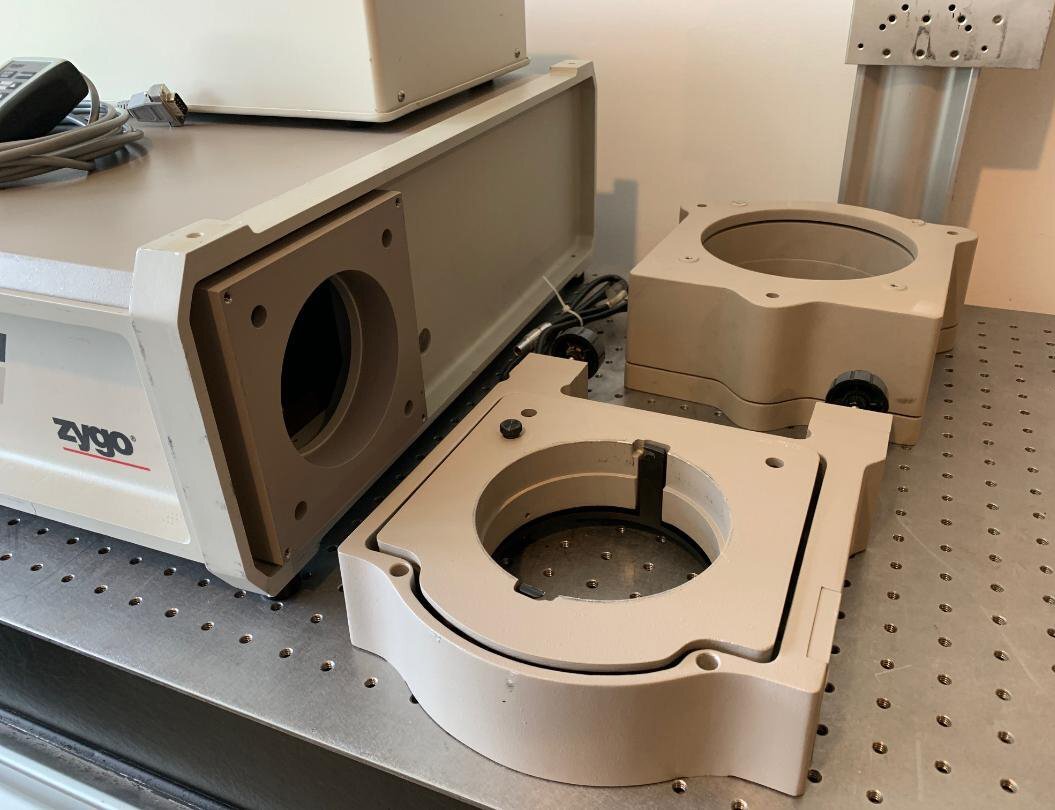
Phase Measuring Receptacle (PMR)
Kinematic tilt tip reference flat mount
Handheld controller
No computer
Cables.
ZYGO Mark GPI-XPS is a mask & wafer inspection equipment designed specifically for advanced photomask and wafer inspection applications. The system uses patent-pending post-processing techniques to maximize the result quality in terms of resolution, accuracy, and speed, making it an ideal choice for inspection of large arrays of small, complex patterns. The unit is equipped with two cameras for full-field imaging. The first camera can be used for brightfield inspection and the second camera for dark field imaging. The image resolution is 1.2 µm, making it ideal for high-resolution wafer and mask inspection. Mark GPI-XPS is able to inspect wafers up to 225 mm in diameter - larger than typical 200 mm wafer inspection systems - making it well-suited for process leak checkers. The machine also features a high-compression, low-noise imaging design for both cameras. This design helps to reduce overall noise levels and produces higher quality images. The tool is also equipped with a high-end illuminator to provide precision lighting for a wide range of inspection requirements. ZYGO Mark GPI-XPS also features pattern matching algorithms to compare results to a database of reference images. The asset searches for features that match predetermined criteria and then identifies them as identical and distinct. This automated procedure helps to identify potential defects with greater accuracy and reduces false positives. Mark GPI-XPS also offers users an intuitive graphical interface for mask and wafer inspection. This user-friendly interface helps operators to quickly set up the model and make mask and wafer inspections. The interface also provides easy-to-understand results with automated defect detection tools that allow users to quickly identify anomalies. ZYGO Mark GPI-XPS is an ideal equipment for photomask and wafer inspection applications. Its features combine to provide high resolution imaging, automated defect detection, and intuitive operation to help enhance yields and optimize process stability. The system is ideal for a wide range of inspection requirements and is sure to provide reliable results.
There are no reviews yet
