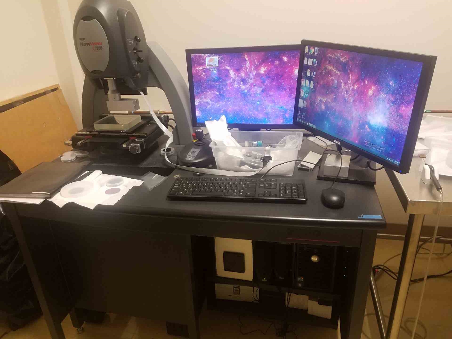
Used ZYGO NewView 7300 #9248752 for sale
It looks like this item has already been sold. Check similar products below or contact us and our experienced team will find it for you.
Tap to zoom


Sold
ID: 9248752
Vintage: 2011
3D Optical profiling system
X, Y Table: 6"
Part no / Description
6300-0459-01 / Electronics, power supply: 110 / 120 VAC, base system included
6450-0815-03 / 7000 Motorized, 5-Axis base stage includes motorized Tip / Tilt, X, Y, Z
6300-0650-01 / Motorized turret (4-Pos) (NV600 / 700 / 6000 / 7000)
6300-0522-02 / 0.5X Field zoom lens
6300-0316-01 / 1x Michelson objective (NV 6000/7000) (Not Turret Mountable)
6300-0593-01 / Objective: 5x Michel son objective
6300-0595-01 / Objective: 20x AF Objective
1776-666-012 / SiC Precision reference flat, 30 mm
1776-666-009 / Step height standard 85 mm
1840-700-105 / Vibration isolation table with 6300-2080-01 workstation table
6301-0401-01:
7300 3D Optical profiling system
Automated 3-position multiple system zoom
With 1.0x lens high performance digital
Closed loop piezo scanning transducer with capacitive feedback
150 Micron scan high speed measurement module
Enhanced illuminator with long lite LED high speed
High resolution CCD camera (640x480) 20 mm extended
Windows XP professional dell OptiPlex 745 minitower
Core 2 Duo 1.86 GHz
(2) DELL USB Keyboards
(2) DELL USB Buttons
Mouse with scroll DELL UltraSharp flat panel monitor, 17" (1.0 GB)
Digital video adapter card: 667 MHz DDR2 2 x 512
SATA Hard Disk Drive (HDD): 80GB
Optical filler panel: 48 X 32 CDRW / DVD
SATA Combo drive
Black PS2 serial port adapter
2011 vintage.
ZYGO NewView 7300 is a mask and wafer inspection equipment that uses advanced optical imaging technology and image processing algorithms to detect and characterize defects on masks and wafers. It is designed to help improve the precision and accuracy of semiconductor production processes and can be used for both 2D and 3D defect inspections. The system works by using an adjustable laser beam to scan a sample surface of a mask or wafer. The laser beam gets reflected off the sample surface and is detected by high-resolution detectors. The detected information is then sent to a high-end image processor for further processing. The image processor then extracts defect detections, characterizes them, and produces a detailed report of the findings. ZYGO NEW VIEW 7300 comes with advanced defect characterization capabilities including the ability to capture, analyze and compare data from multiple fields of view of the sample surface and detect even small defects. It also offers reliable imaging for nanometer-level letter and logic inspections. NewView 7300 is well-suited for applications such as wafer and mask inspection, wafer and mask qualification, and defects detection in die side imaging. It offers a comprehensive suite of features, including a dynamic focus unit to ensure greater accuracy, dual-band laser illumination technology for enhanced contrast, and a high-speed laser scanning machine for faster processing of high-resolution images. It is equipped with a powerful image processing engine and advanced analysis capabilities to enable accurate inspection and characterization of defects and their precise location. The tool can also be integrated with SEM/TEM instruments for automated sample verification and delivery of defect data. NEW VIEW 7300 comes with a user-friendly, intuitive graphical user interface for easy setup and operation. The asset is designed to meet the highest standards of accuracy and reliability; contributes to optimal manufacturing process yields; and can be used in a wide range of semiconductor production options.
There are no reviews yet