Used ABM Mask aligner #293824118 for sale
URL successfully copied!
Tap to zoom

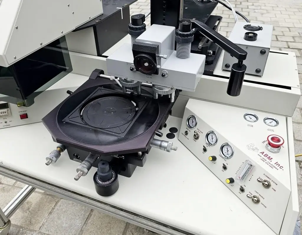
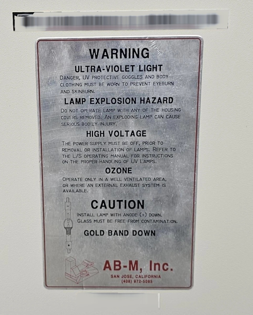
ID: 293824118
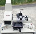
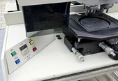
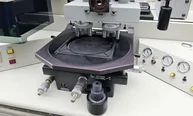
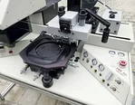
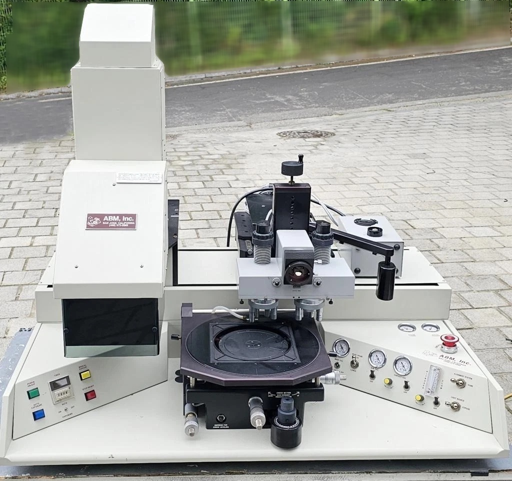
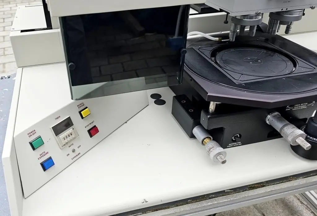
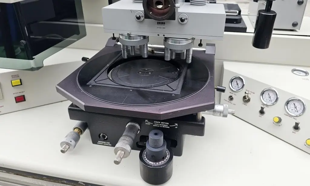
ABM Mask Aligner is a cutting-edge wafer processing equipment designed for high-precision and reliable photolithography applications in semiconductor manufacturing and microelectronics industries. This advanced equipment plays a crucial role in patterning photomasks onto silicon wafers with exceptional accuracy, enabling the creation of intricate microstructures and circuits essential for integrated circuits (ICs), MEMS devices, sensors, and photonics devices. Mask Aligner leverages sophisticated optical alignment technology to ensure precise overlay between the photomask and the wafer during the exposure process. This alignment capability is crucial for achieving submicron resolution and feature sizes, which are essential for next-generation semiconductor devices with increasing complexity and shrinking dimensions. Key features of ABM Mask Aligner include a robust and stable mechanical platform, a high-resolution imaging system, and user-friendly software interfaces for efficient operation and process control. The unit typically consists of a stage for holding the wafer, a stage for the photomask, a high-intensity light source (such as UV or deep UV), an optical machine for alignment and focusing, and sophisticated control electronics to manage the exposure parameters. One of the primary functions of Mask Aligner is to transfer the pattern on the photomask onto the wafer through a photolithography process. This involves coating the wafer with a photosensitive material called photoresist, placing the photomask on top of the wafer, aligning them accurately using the alignment tool, and exposing them to UV light through a series of precise control steps. During exposure, the light passes through the transparent regions of the photomask, exposing the underlying photoresist on the wafer. The photoresist undergoes a chemical reaction upon exposure, creating a patterned mask that can be developed and etched to transfer the pattern onto the wafer surface. ABM Mask Aligner offers several advantages over traditional contact and proximity aligners, including higher resolution, improved overlay accuracy, reduced proximity effects, and enhanced process control. These capabilities are particularly crucial for advanced semiconductor technologies, such as sub-10nm nodes, where the alignment and pattern fidelity requirements are extremely stringent. Moreover, Mask Aligner is equipped with intelligent alignment algorithms and motorized stages that enable automatic alignment and exposure, reducing operator error and increasing throughput in production environments. The asset's software interface allows users to define exposure parameters, monitor alignment accuracy, and analyze process data for optimization and quality control purposes. In conclusion, ABM Mask Aligner represents a state-of-the-art solution for wafer processing and photolithography applications in the semiconductor industry. Its advanced features, precision performance, and user-friendly interface make it an indispensable tool for fabricating next-generation ICs and microelectronic devices with unparalleled accuracy and reliability.
There are no reviews yet