Used AMAT / APPLIED MATERIALS / ADLINK CPCI-3615FEP #293820241 for sale
URL successfully copied!
Tap to zoom
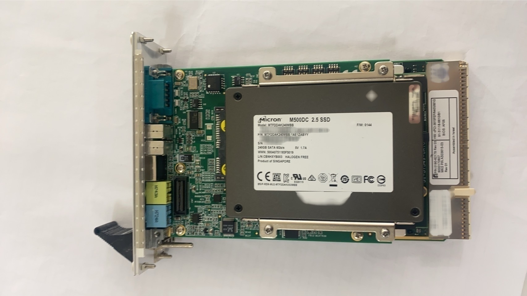

ID: 293820241
3U CCI Processor board
MICRON M500DC SSD, part number: MTFDDAK24DMBB-1AE1ZABYY.
AMAT / APPLIED MATERIALS / ADLINK CPCI-3615FEP is a cutting-edge wafer processing equipment designed for the semiconductor and microelectronics industry. This system is a crucial component in the fabrication process of integrated circuits, chips, and other electronic devices. As a SEO specialist, it is important to understand the technical aspects and functionalities of these systems to effectively create content that resonates with the target audience. AMAT CPCI-3615FEP is manufactured by AMAT, a leading provider of equipment, services, and software to the semiconductor industry. This unit integrates advanced technologies and features to deliver high-performance wafer processing capabilities. It is specifically designed for Front-End Processing (FEP) applications, which involve key processes such as deposition, etching, and cleaning of semiconductor wafers. One of the key features of ADLINK CPCI-3615FEP is its CompactPCI (CPCI) form factor, which offers a compact and modular design suitable for integration into semiconductor manufacturing environments. This design allows for easy scalability and flexibility in machine configurations, making it well-suited for both research and production settings. The tool is equipped with advanced control and monitoring capabilities that ensure precise and reliable wafer processing. It utilizes sophisticated software algorithms to manage the various process parameters, such as temperature, pressure, and gas flow rates. This level of control is essential for achieving consistent and high-quality processing results. In terms of processing capabilities, CPCI-3615FEP offers a wide range of functions to support different wafer processing requirements. It is capable of performing various deposition techniques, including chemical vapor deposition (CVD) and physical vapor deposition (PVD), to create thin film layers on the wafer surface. Additionally, the asset can carry out etching processes to selectively remove material from the wafer to create intricate circuit patterns. Furthermore, APPLIED MATERIALS CPCI-3615FEP incorporates advanced cleaning methodologies to ensure the cleanliness and purity of the wafer surfaces. This is crucial for preventing contaminants and defects that can negatively impact the performance and reliability of the final semiconductor devices. The model is also designed for high-throughput processing to meet the demanding production requirements of semiconductor fabrication facilities. It features efficient wafer handling mechanisms, such as robotic arms and vacuum chambers, to streamline the processing workflow and minimize downtime. Overall, AMAT / APPLIED MATERIALS / ADLINK CPCI-3615FEP represents a state-of-the-art solution for wafer processing in the semiconductor industry. Its advanced technologies, compact design, and versatile capabilities make it an essential tool for achieving high-quality and cost-effective semiconductor manufacturing. Understanding the technical details and functionalities of this equipment is crucial for effectively communicating its value proposition to the target audience in the semiconductor and microelectronics sector.
There are no reviews yet