Used AMAT / APPLIED MATERIALS Chambers #293813909 for sale
URL successfully copied!
Tap to zoom

ID: 293813909
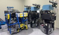
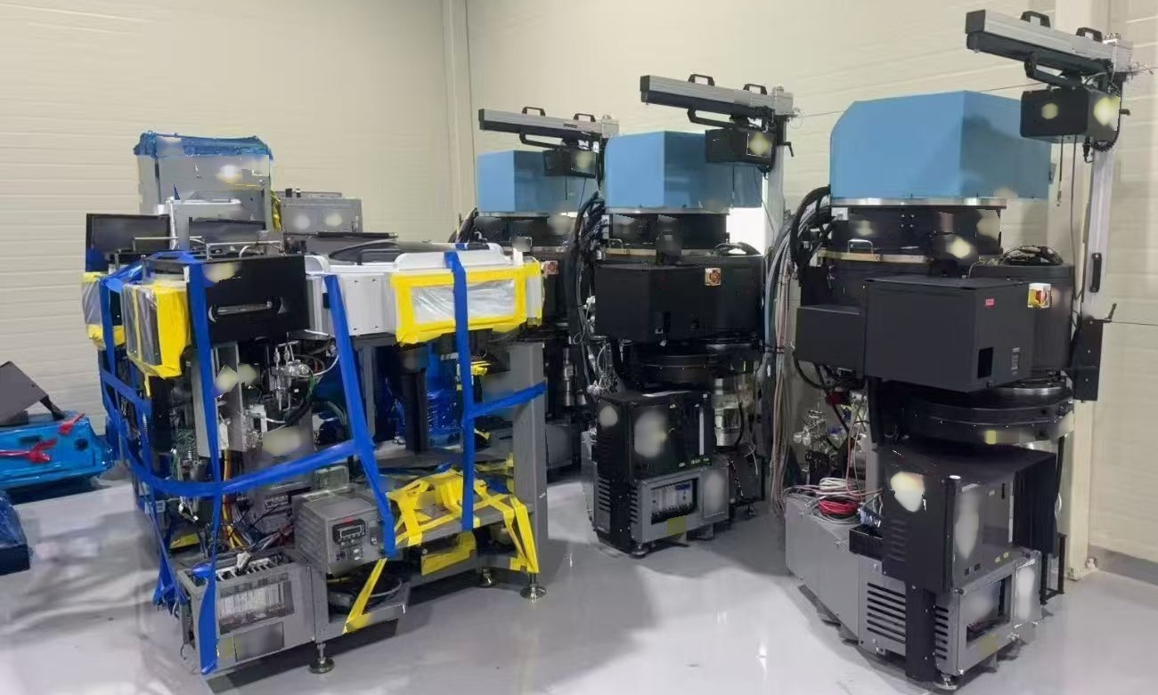
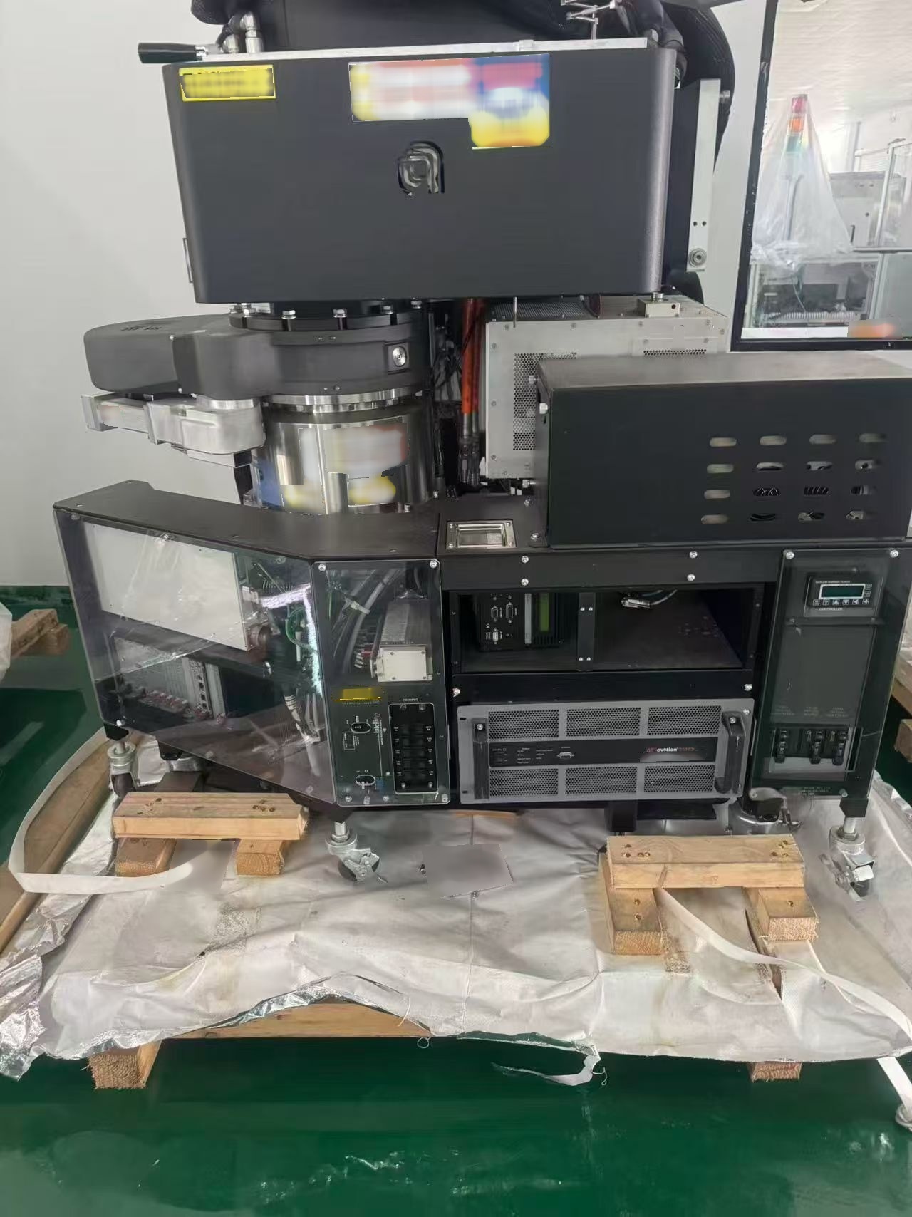
AMAT / APPLIED MATERIALS Chambers are an integral component of the wafer processing system utilized in semiconductor manufacturing. These AMAT Chambers serve as essential environments for executing various processes involved in wafer fabrication, including deposition, etching, and cleaning. Created by AMAT Inc., a leading global provider of equipment, services, and software for the semiconductor, flat panel display, and solar photovoltaic industries, APPLIED MATERIALS Chambers are known for their high quality, precision, and reliability in delivering consistent and efficient results. Chambers are designed to provide a controlled atmosphere that is free of contaminants and has the necessary conditions for carrying out advanced semiconductor processes. Each chamber is equipped with sophisticated technology and features to support specific fabrication steps, ensuring optimal performance and productivity. These AMAT / APPLIED MATERIALS Chambers are often part of a larger wafer processing system, working in conjunction with other components such as robotics, handling systems, and monitoring devices to enable the seamless execution of wafer manufacturing processes. One of the primary functions of AMAT Chambers is thin film deposition, which involves depositing materials onto the wafer surface to create thin layers with specific properties. This process is crucial for building the various components of semiconductor devices, such as transistors, capacitors, and interconnects. APPLIED MATERIALS Chambers are designed to accommodate different deposition techniques, including chemical vapor deposition (CVD) and physical vapor deposition (PVD), allowing manufacturers to achieve precise control over film thickness, composition, and uniformity. In addition to deposition, Chambers are also equipped for etching processes, which involve selectively removing material from the wafer surface to create patterns and structures. Etching is essential for defining the features of semiconductor devices and shaping the layers deposited during the fabrication process. AMAT / APPLIED MATERIALS Chambers feature advanced etching technology, such as plasma etching and reactive ion etching, to achieve high levels of precision and selectivity in etching patterns on the wafer. Furthermore, AMAT Chambers include cleaning capabilities to ensure the wafer surface remains free of contaminants and residues that could impair device performance. Cleaning processes such as plasma cleaning and wet cleaning are performed within APPLIED MATERIALS Chambers to maintain wafer integrity and prevent defects during subsequent processing steps. By incorporating advanced cleaning techniques, Chambers help enhance wafer yield and reduce the occurrence of defects in the final semiconductor devices. AMAT / APPLIED MATERIALS Chambers are designed with a focus on reliability, scalability, and flexibility to meet the evolving needs of semiconductor manufacturers. These AMAT Chambers undergo rigorous testing and quality control measures to ensure consistent performance and adherence to industry standards. Moreover, APPLIED MATERIALS Chambers are designed for easy integration into existing wafer processing systems, allowing manufacturers to enhance their production capabilities without disrupting their current operations. Overall, Chambers represent a critical component of the wafer processing system, enabling semiconductor manufacturers to achieve high-quality, high-performance devices through advanced deposition, etching, and cleaning processes. With their innovative technology and precision engineering, these AMAT / APPLIED MATERIALS Chambers play a vital role in driving advancements in semiconductor manufacturing and facilitating the creation of next-generation devices for various applications.
There are no reviews yet