Used MICROSENSE UMA-C200 #293819417 for sale
URL successfully copied!
Tap to zoom
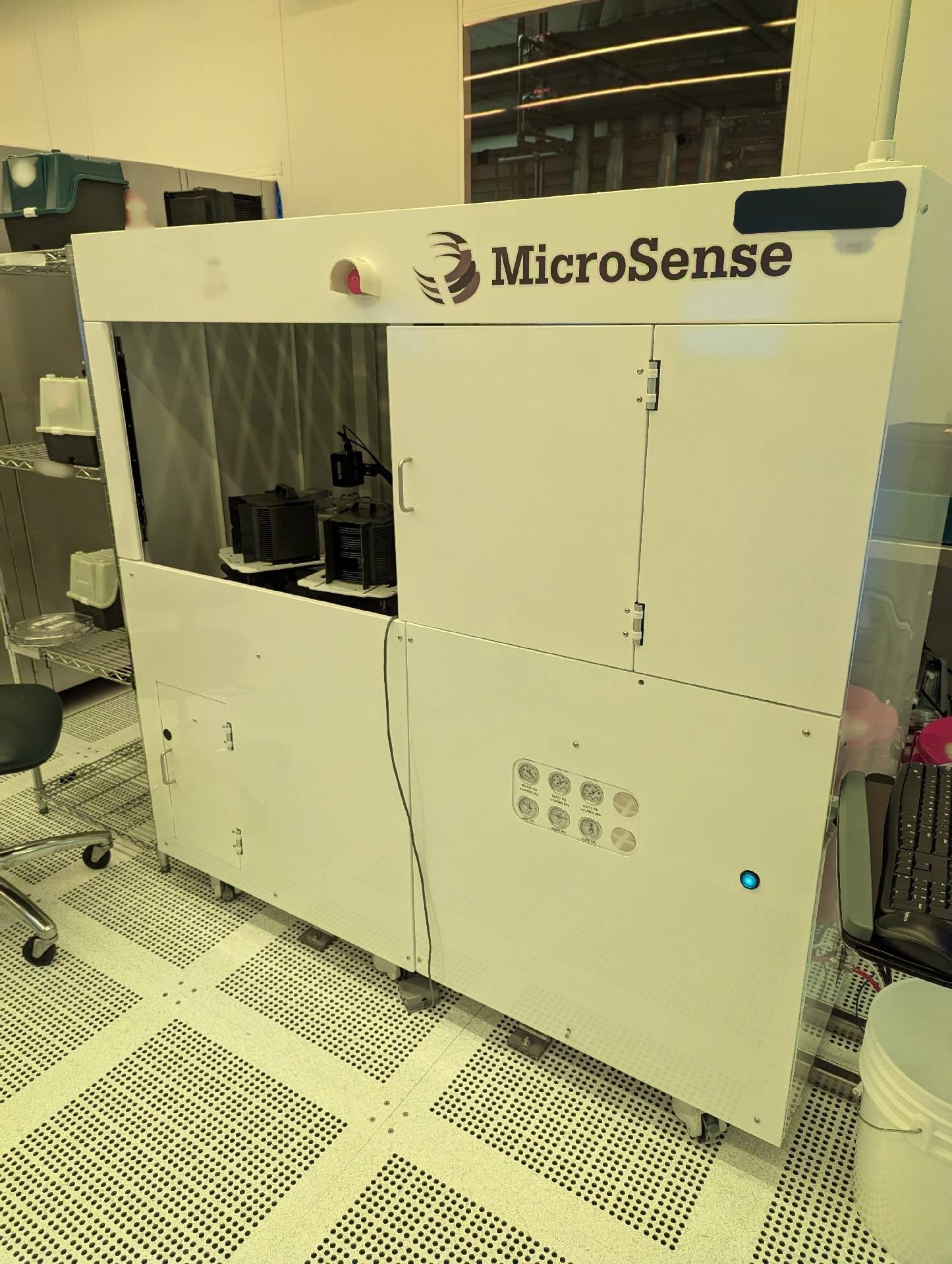

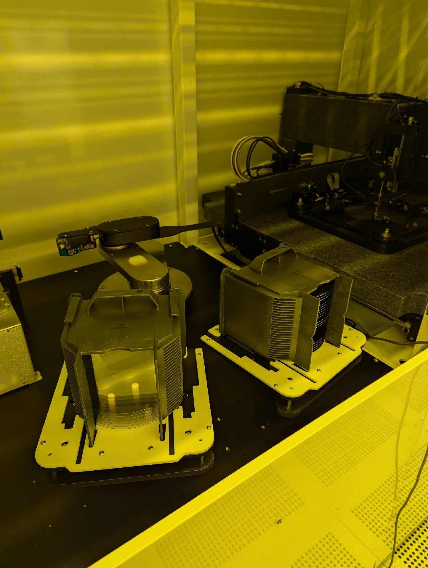
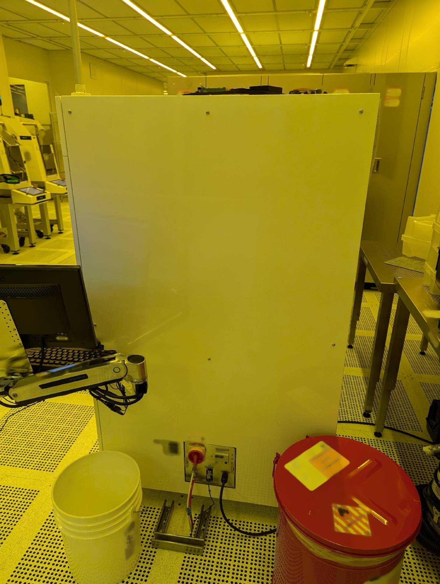
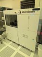
MICROSENSE UMA-C200 is an advanced other wafer processing equipment designed for precise and efficient wafer measurement and characterization in semiconductor manufacturing processes. This innovative system combines state-of-the-art technology with advanced software algorithms to provide accurate and reliable wafer metrology solutions to meet the demanding requirements of the semiconductor industry. At the core of UMA-C200 unit is a high-precision stage that enables the precise positioning of the wafer for measurement and analysis. The stage is equipped with advanced motion control systems that ensure smooth and accurate movements, allowing for the precise positioning of the wafer under the measurement tools. This level of precision is essential for ensuring accurate measurements and reliable results. MICROSENSE UMA-C200 machine features a range of measurement tools and sensors that enable the characterization of various wafer properties, including thickness, flatness, and roughness. These tools are designed to provide high-resolution measurements with sub-micron accuracy, allowing for the detailed analysis of wafer surfaces and properties. Additionally, the tool is equipped with advanced imaging capabilities that allow for the visualization of wafer features and defects in high resolution. One of the key features of UMA-C200 asset is its advanced software platform, which provides powerful data analysis and visualization tools for processing and interpreting measurement data. The software allows users to perform complex data analysis, generate detailed reports, and visualize measurement results in a clear and intuitive format. This enables engineers and researchers to extract valuable insights from the data and make informed decisions about wafer processing and manufacturing processes. MICROSENSE UMA-C200 model is designed to be highly versatile and flexible, allowing for the customization of measurement protocols and procedures to meet specific application requirements. The equipment can be easily integrated into existing semiconductor manufacturing processes and workflows, providing seamless compatibility with other equipment and tools. This flexibility enables users to adapt the system to different measurement tasks and applications, making it a versatile and adaptable solution for a wide range of semiconductor manufacturing processes. In addition to its advanced technical capabilities, UMA-C200 unit is also designed with user convenience and usability in mind. The machine features an intuitive user interface that is easy to navigate and use, allowing users to quickly set up measurement tasks, control the tool, and analyze measurement data. The asset also includes robust safety features and automated procedures to ensure the reliable and safe operation of the equipment. Overall, MICROSENSE UMA-C200 is a cutting-edge other wafer processing model that combines precision, versatility, and user-friendliness to provide a comprehensive solution for wafer metrology in semiconductor manufacturing. With its advanced technology, powerful software platform, and flexible design, UMA-C200 equipment offers semiconductor manufacturers a reliable and efficient solution for wafer measurement and characterization, helping to improve the quality, efficiency, and yield of semiconductor manufacturing processes.
There are no reviews yet