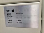
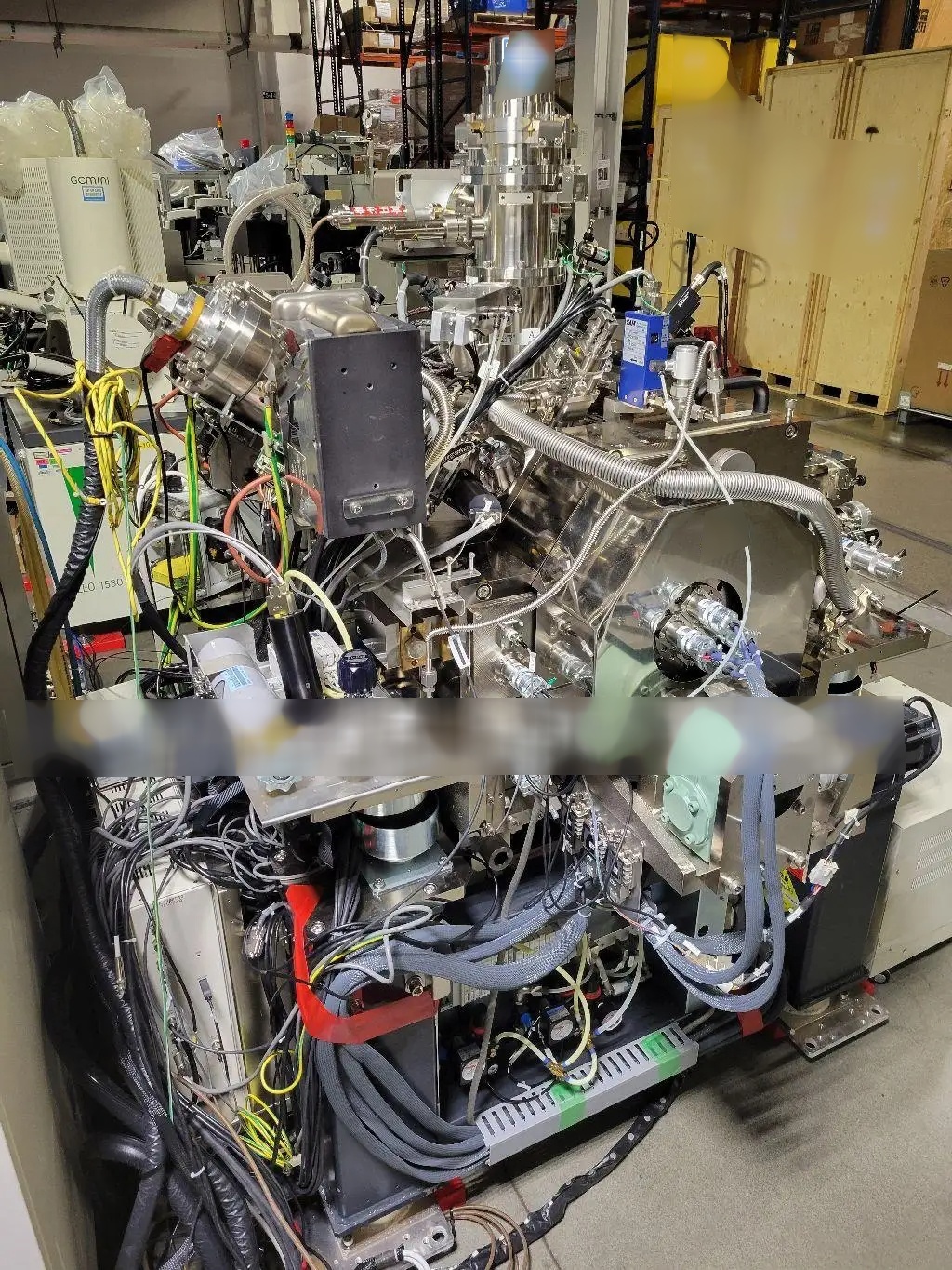
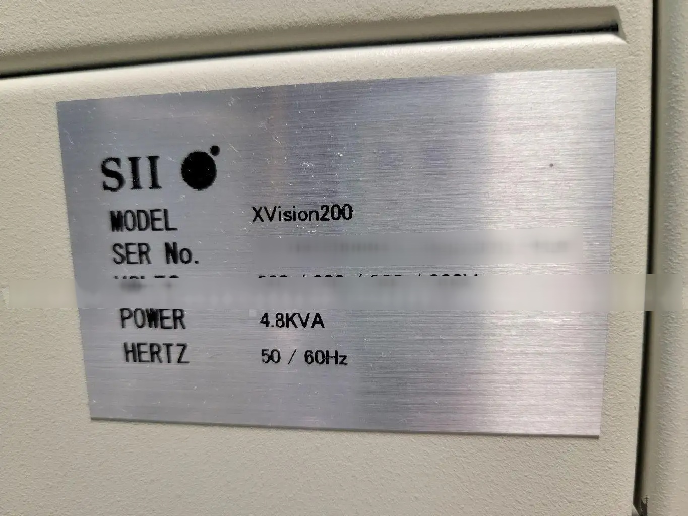
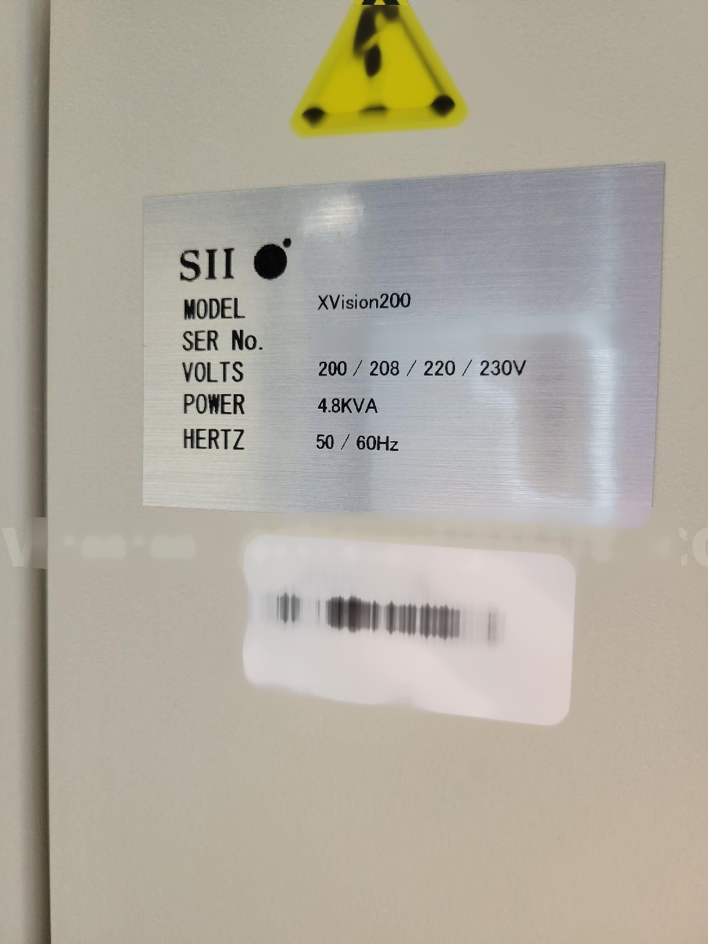
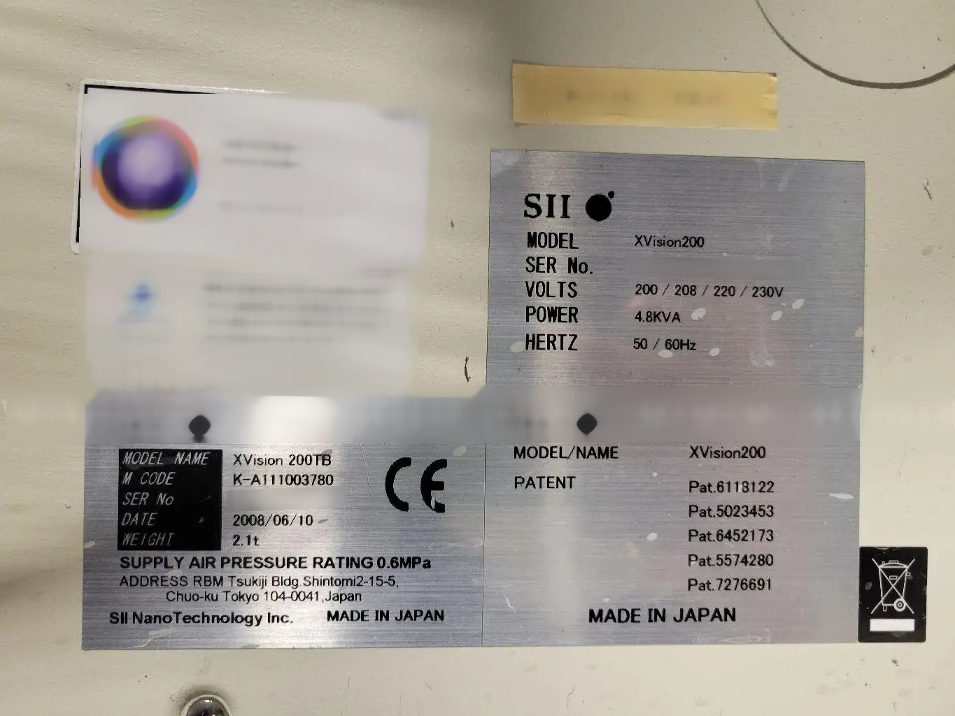
Used SII NANO TECHNOLOGY X-Vision 200TB #293824625 for sale
URL successfully copied!

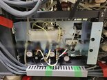
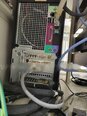
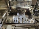
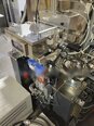


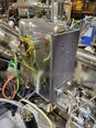







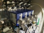
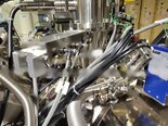
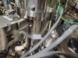
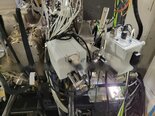



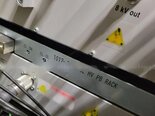
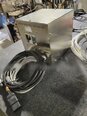
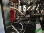






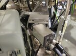
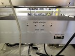
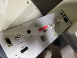

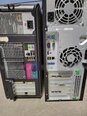

Tap to zoom

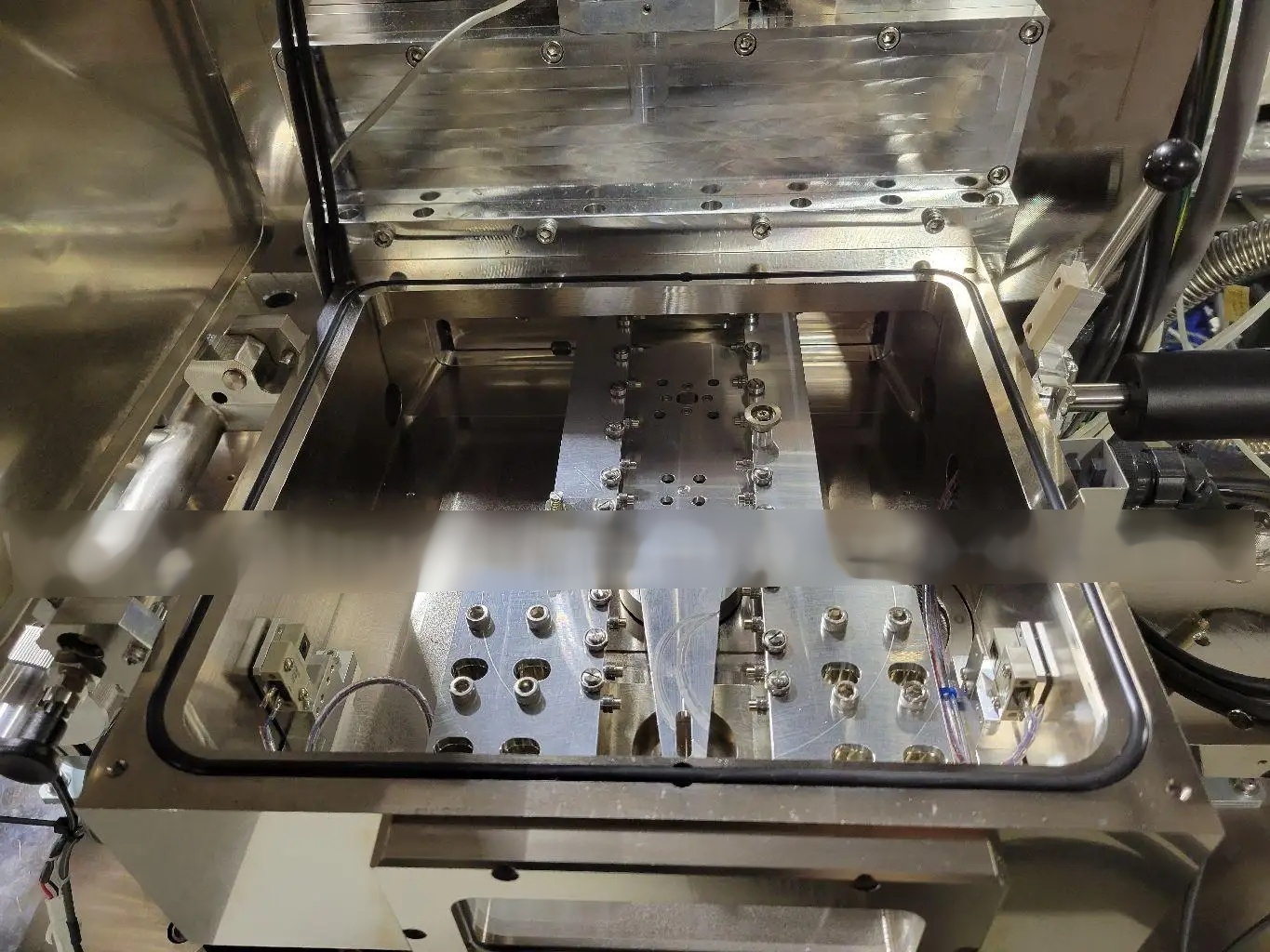
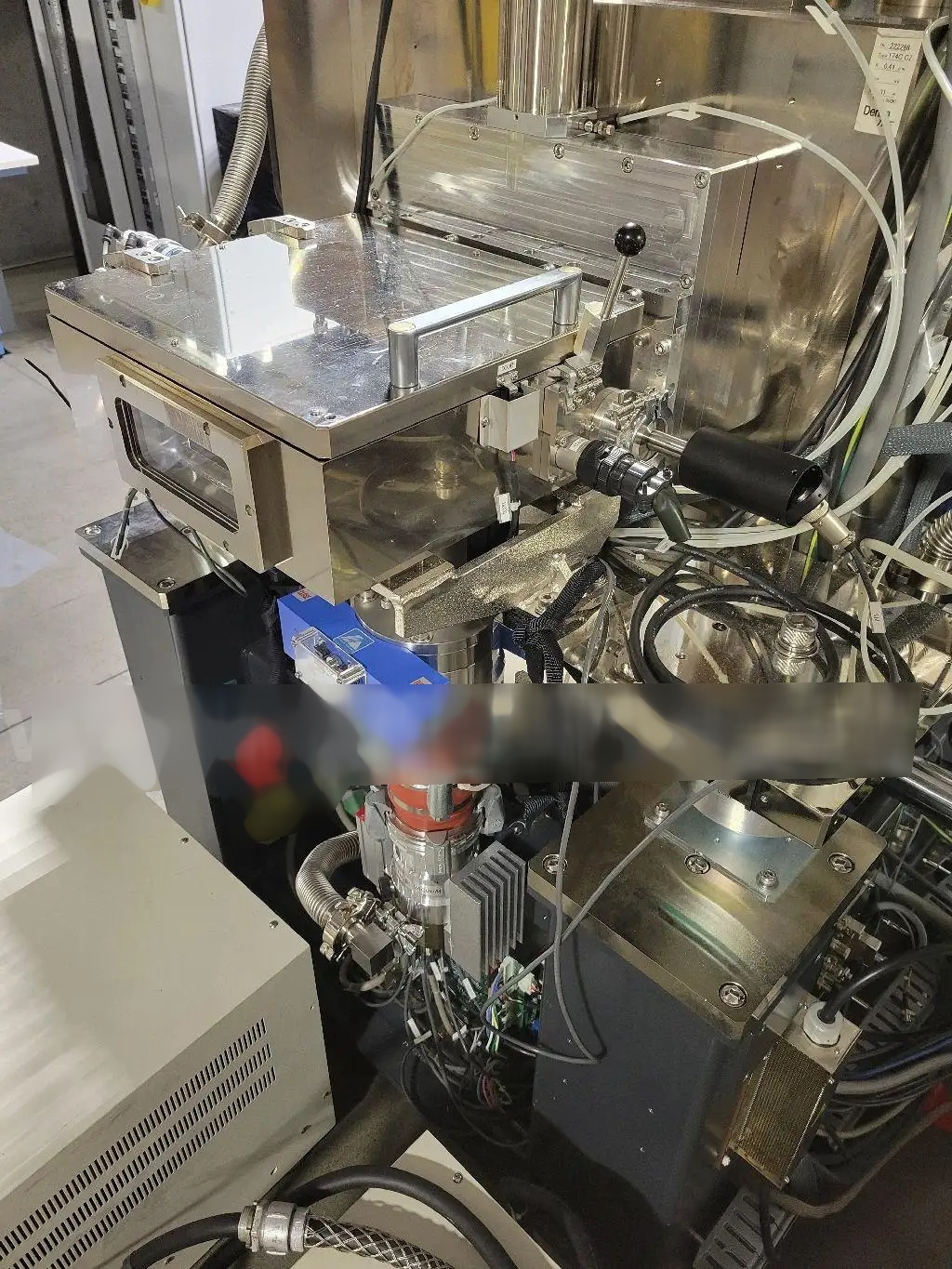
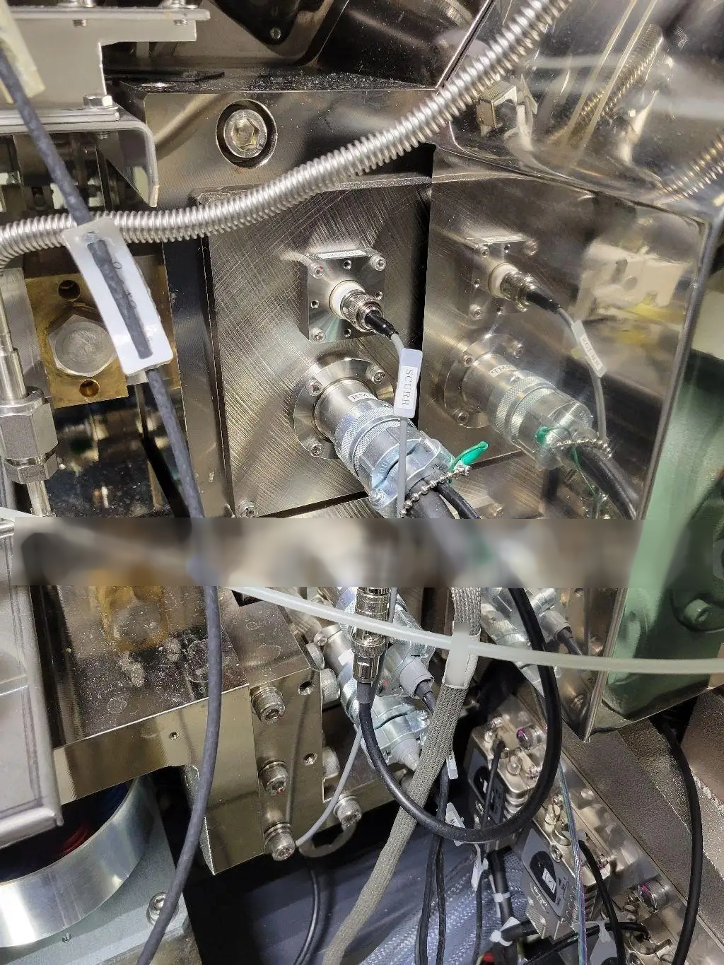
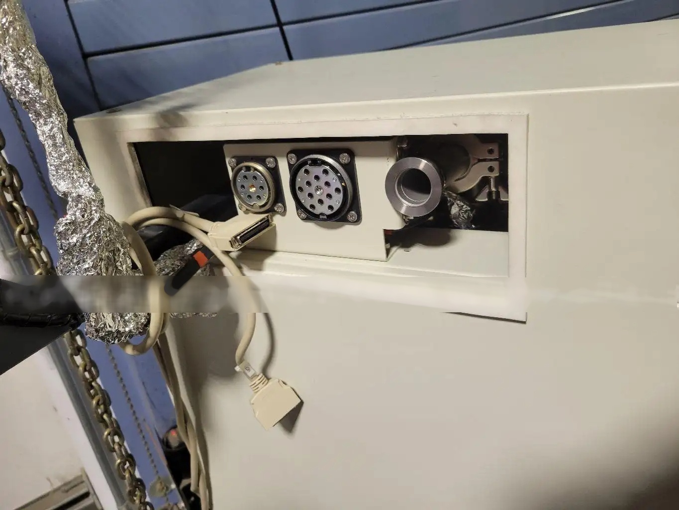
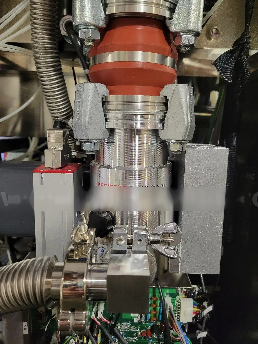
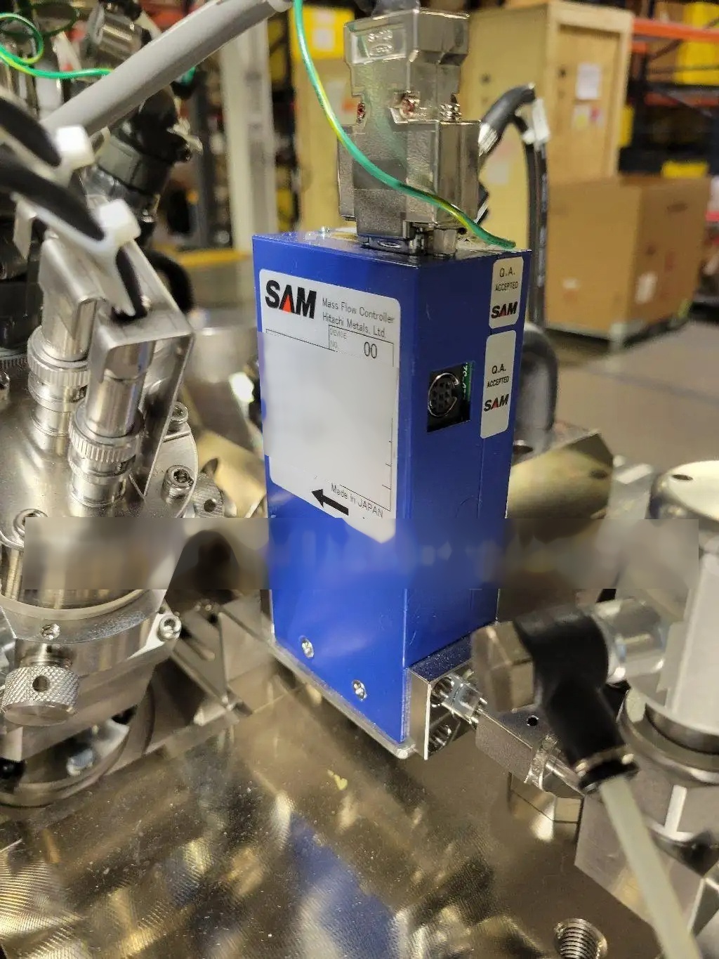
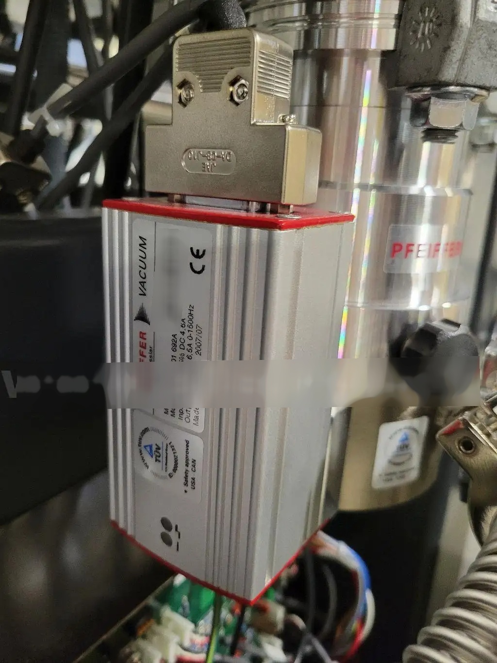
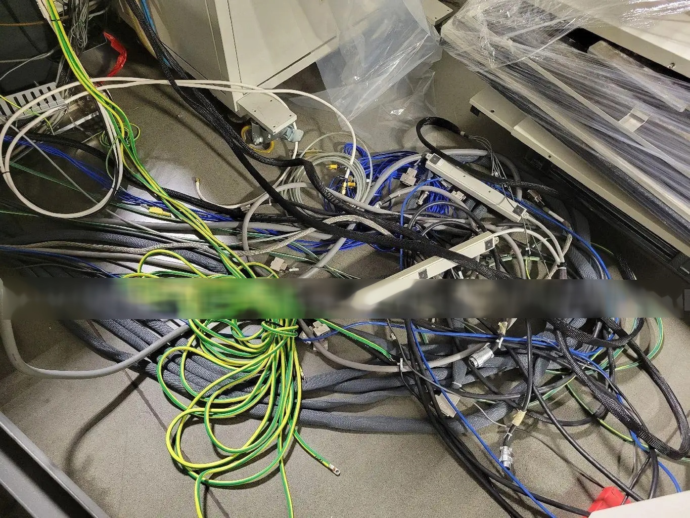
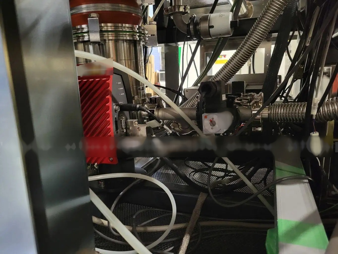
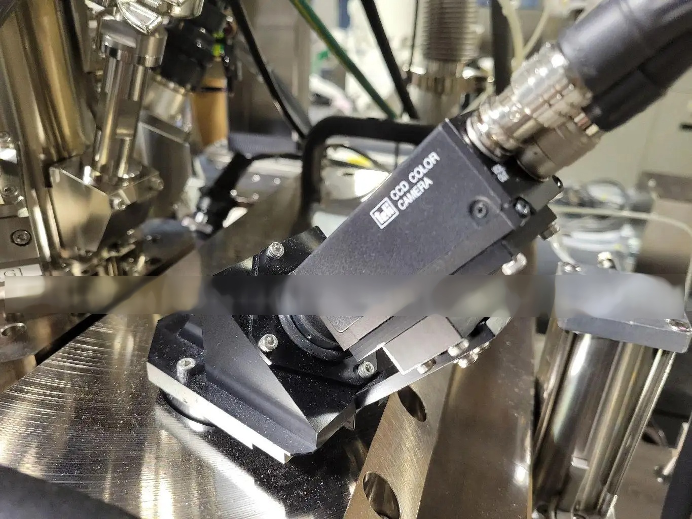
ID: 293824625
Vintage: 2008
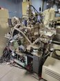
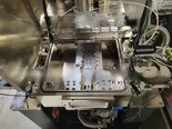
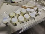
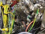
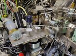
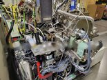
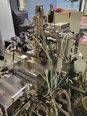
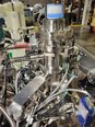
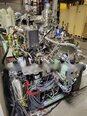
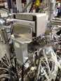
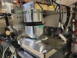
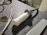
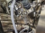
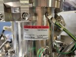
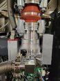
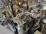
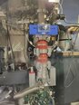
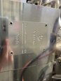
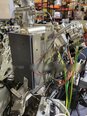
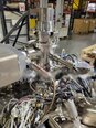
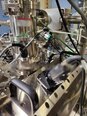
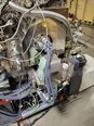
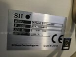
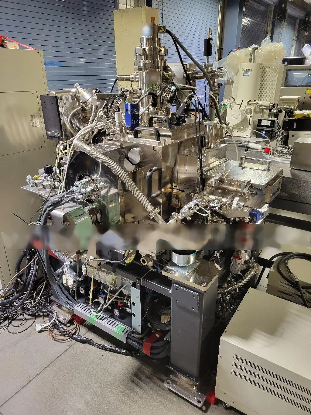
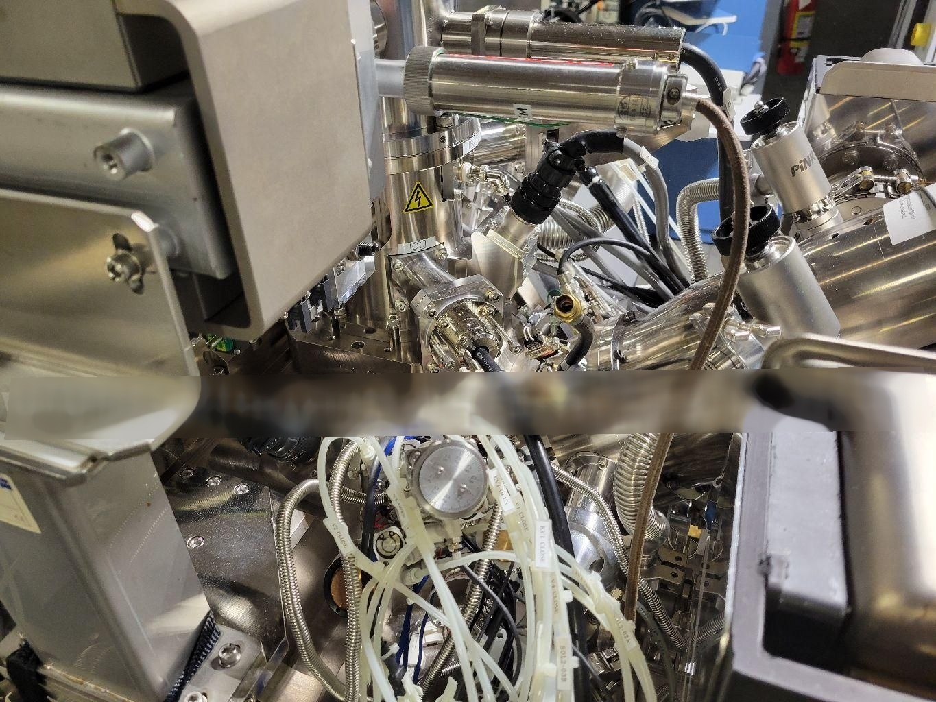
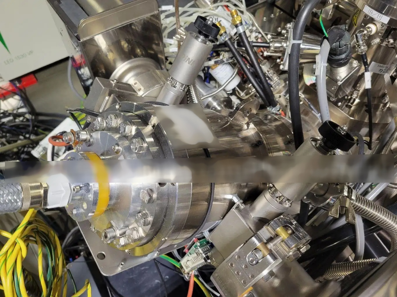
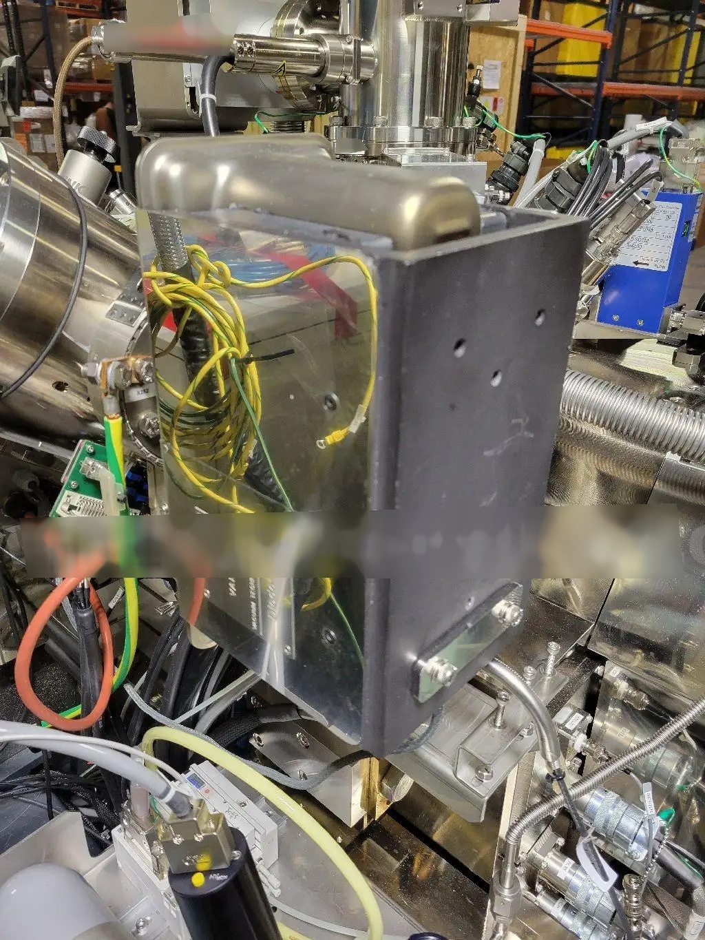
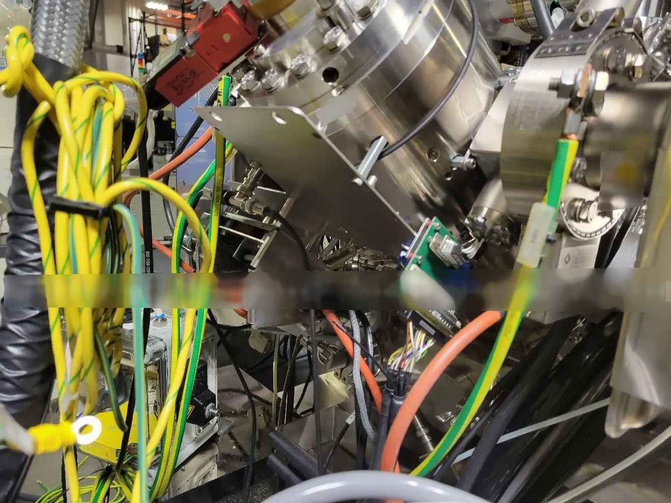
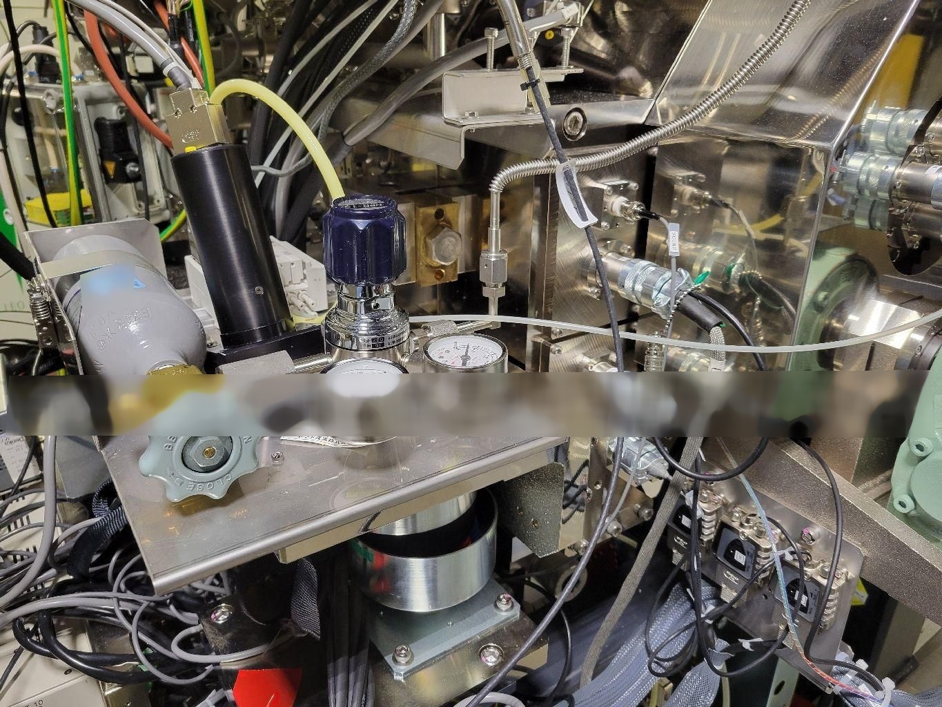
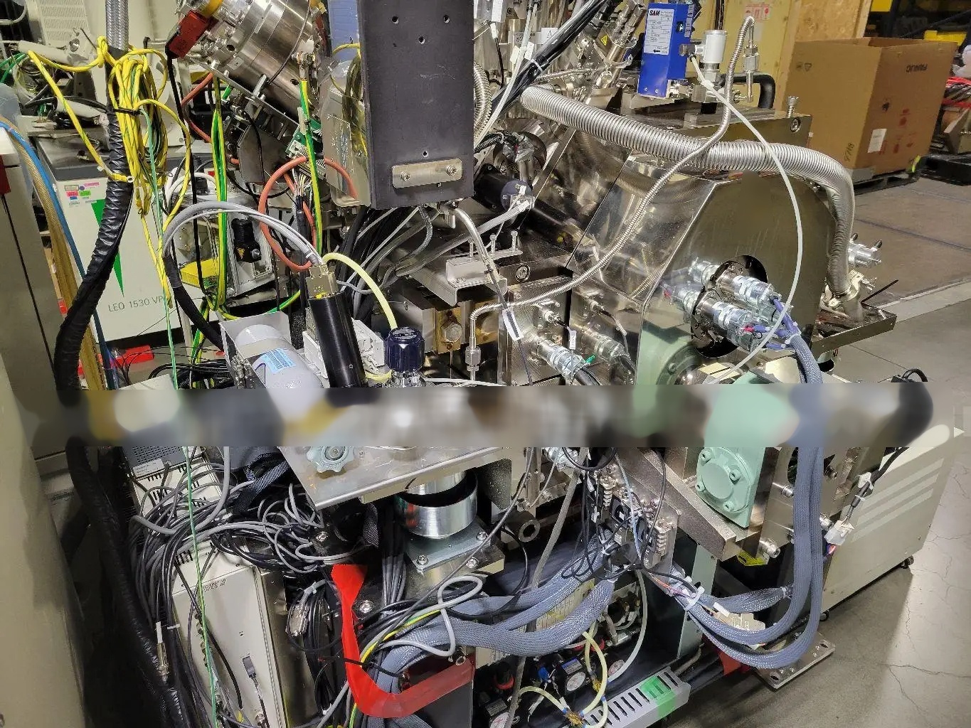
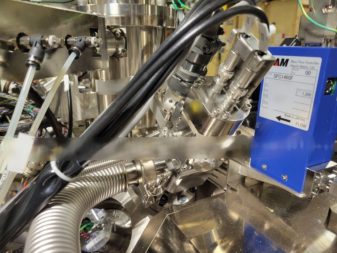
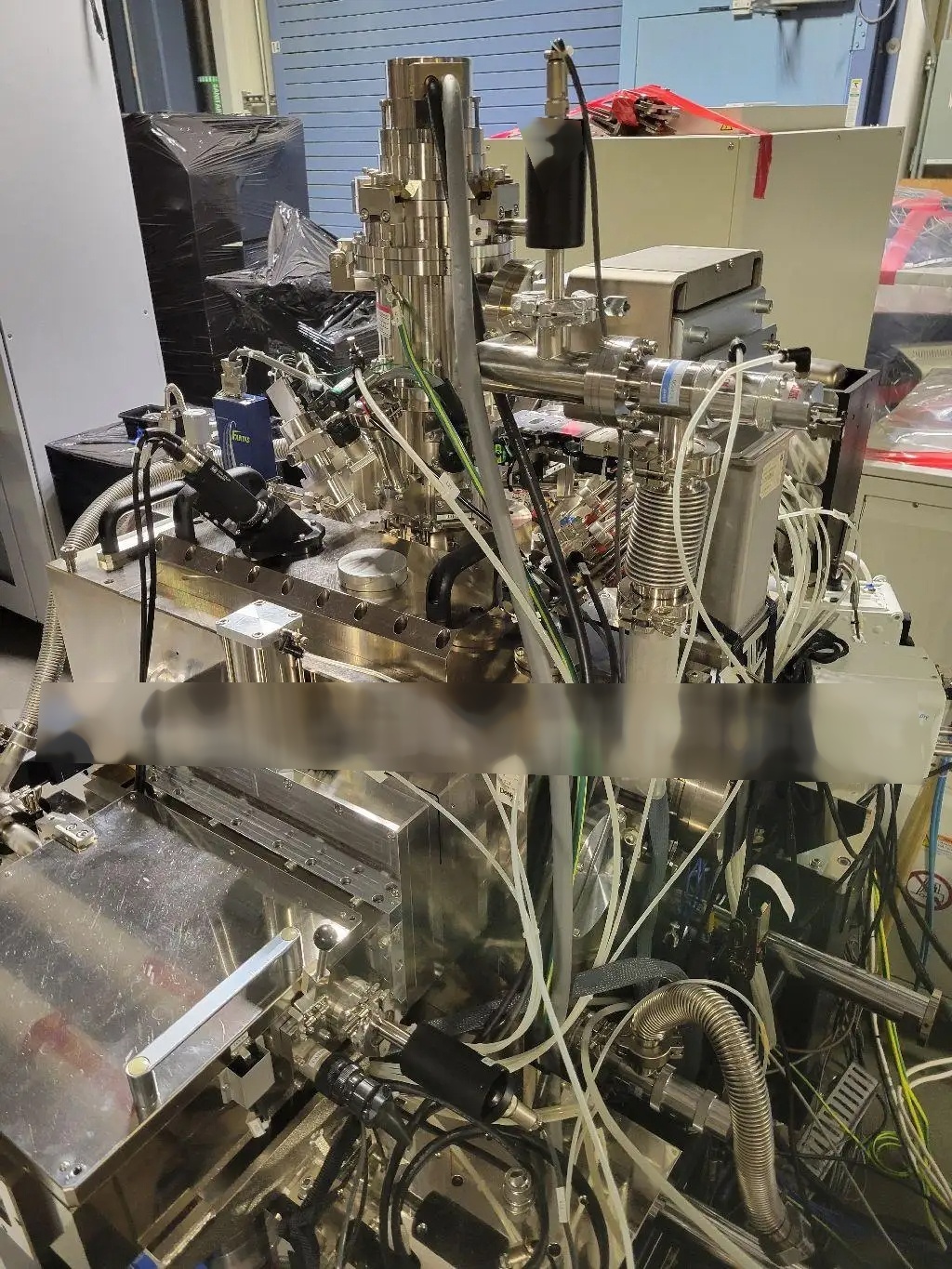
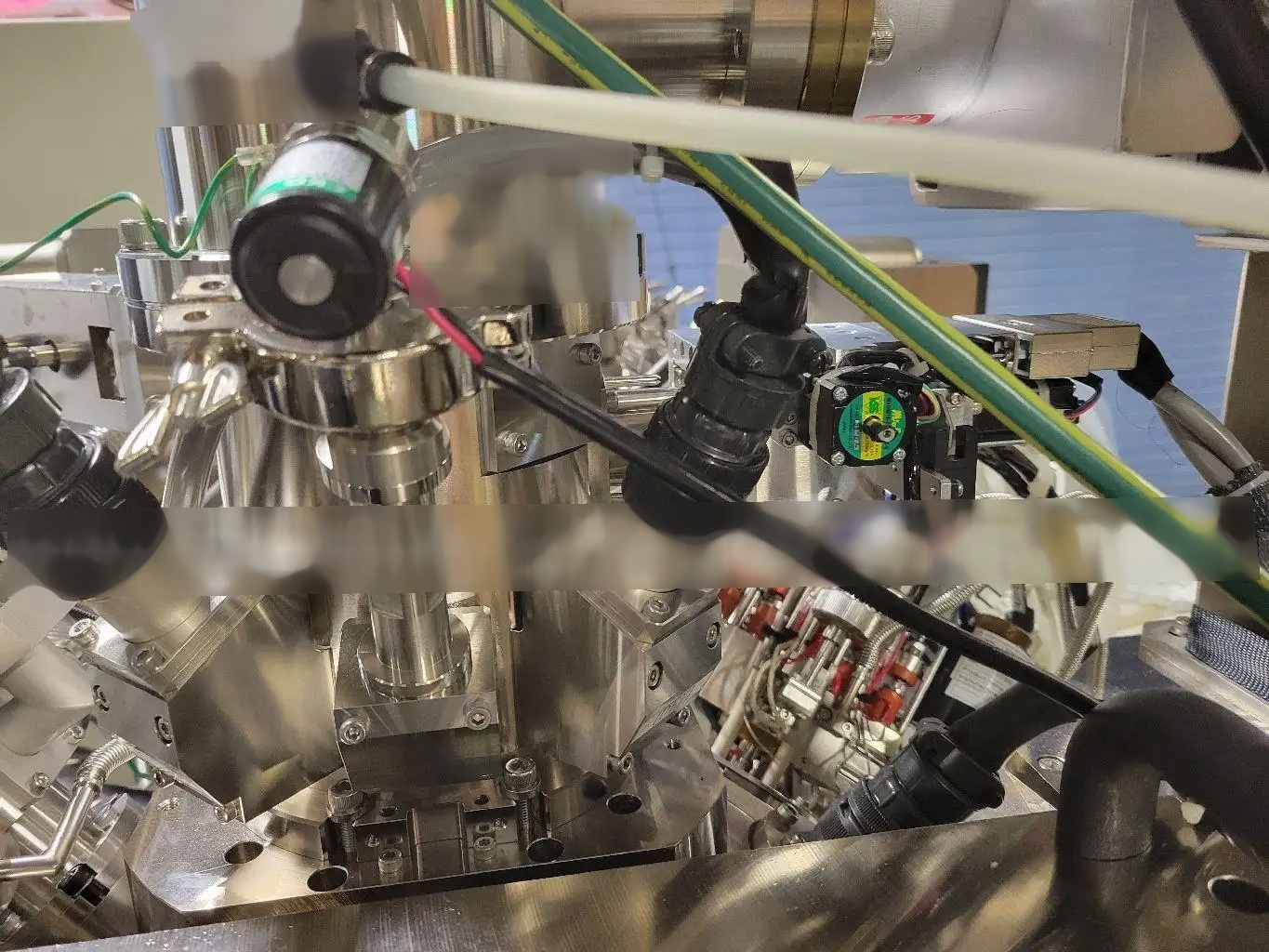
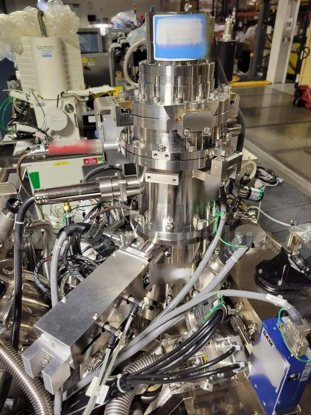
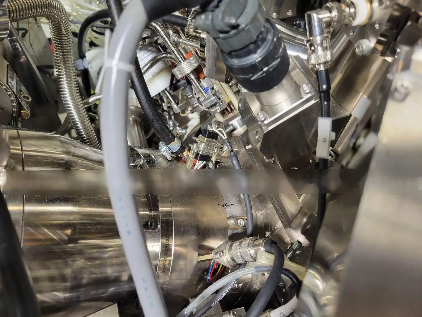
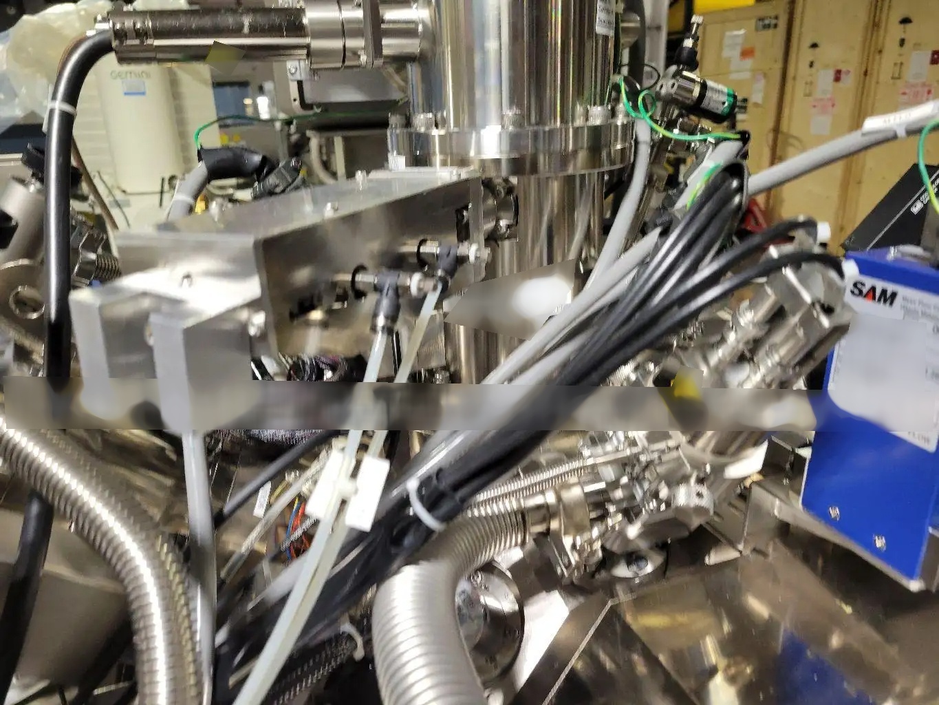
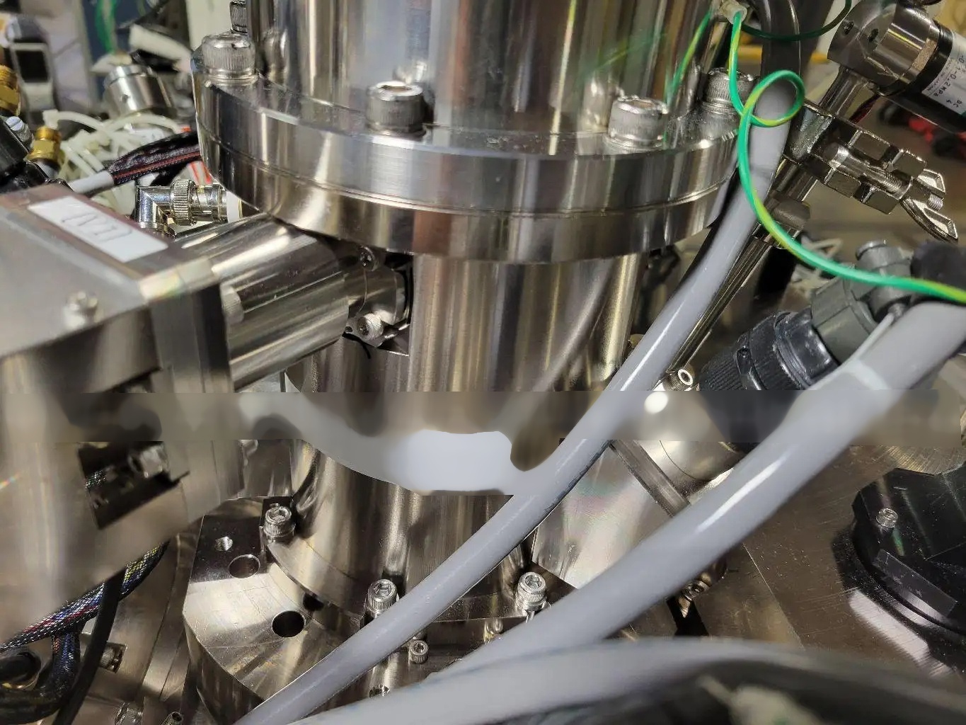
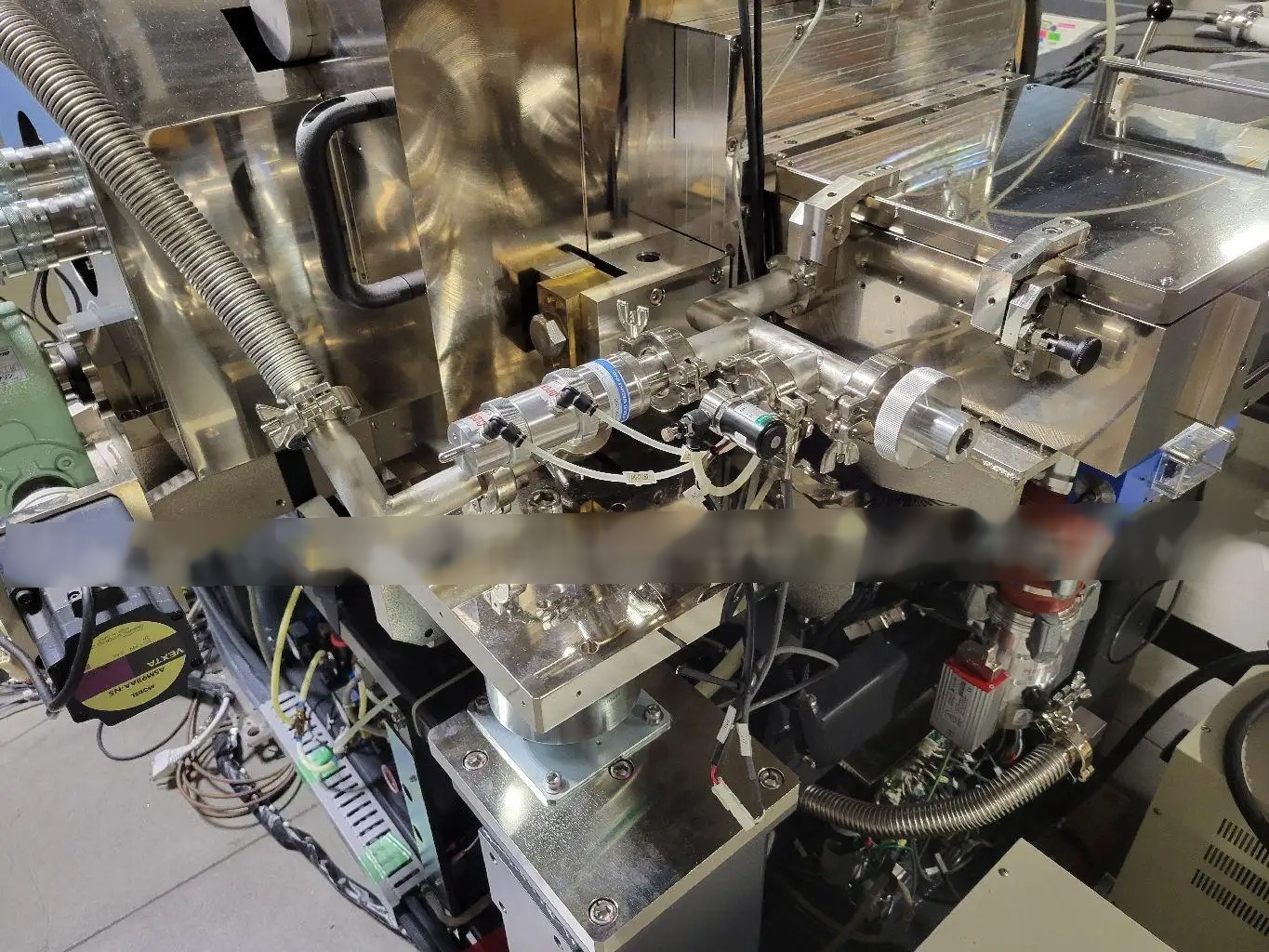
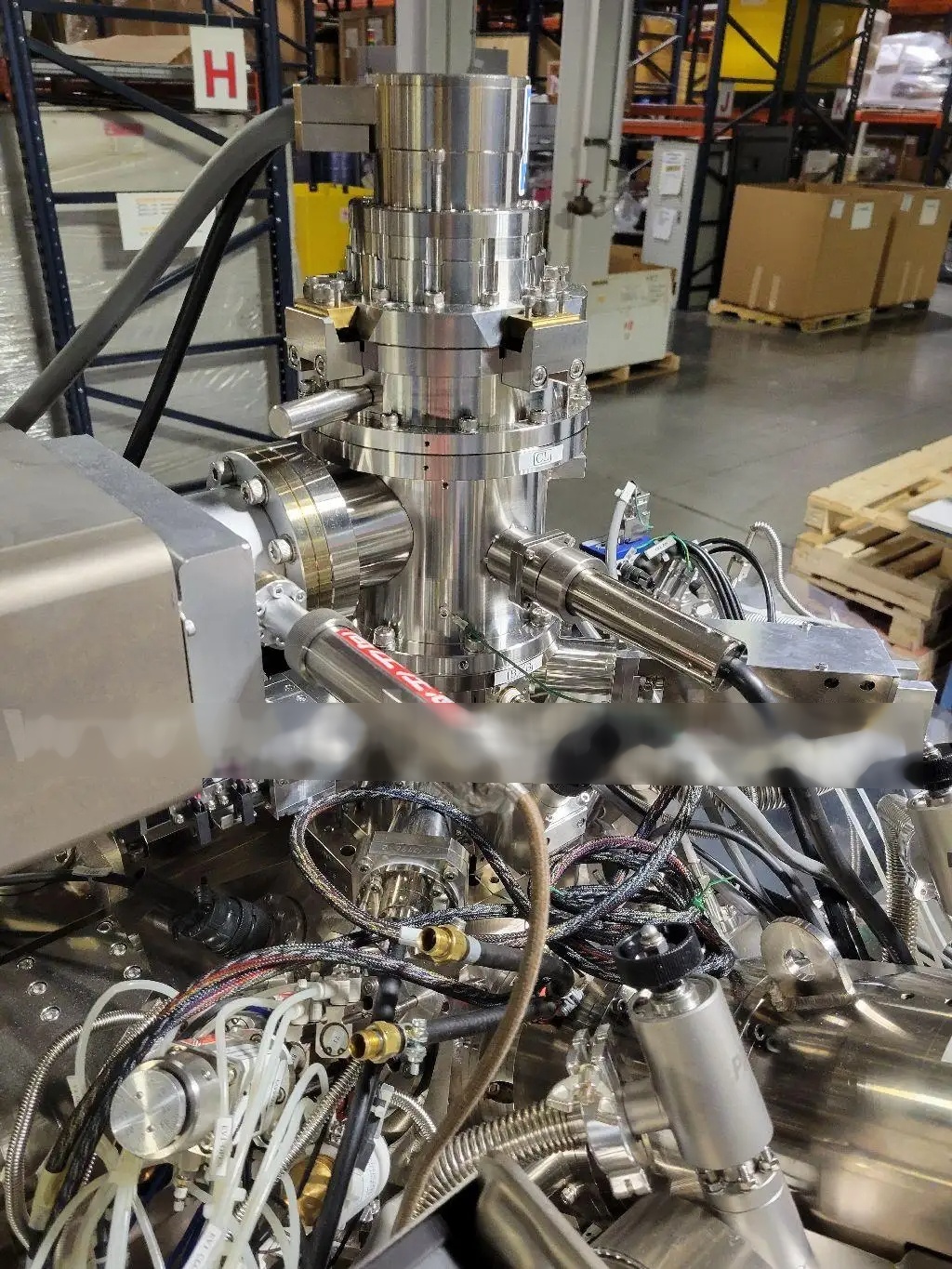
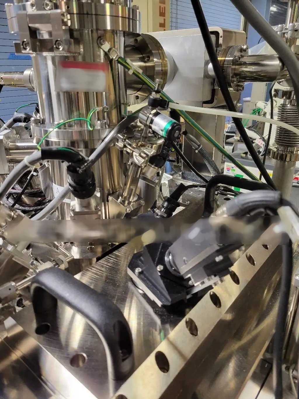
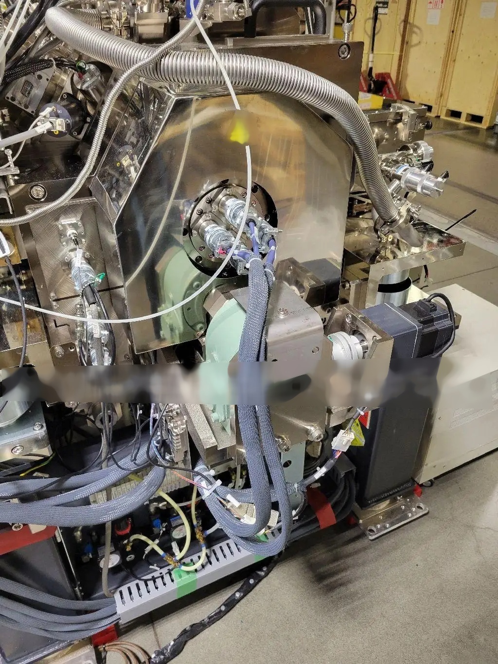
FIB-SEM System
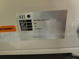
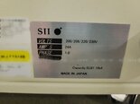
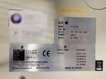
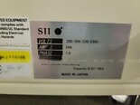
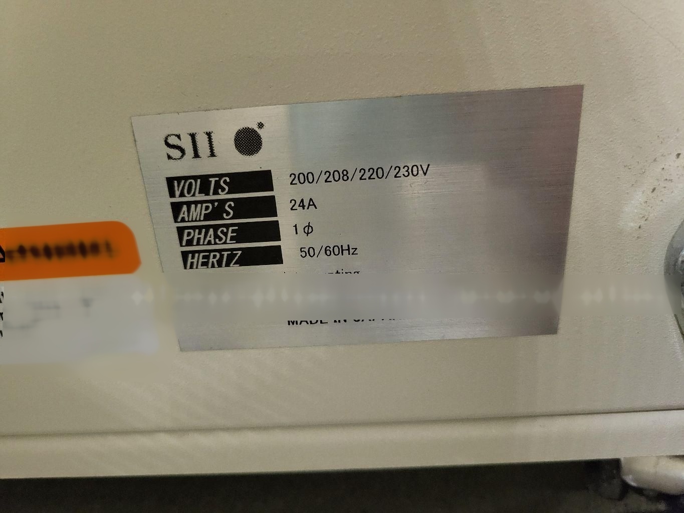
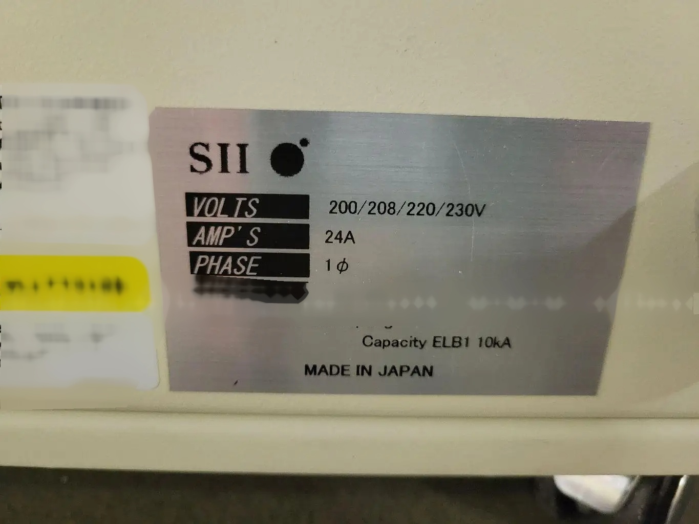
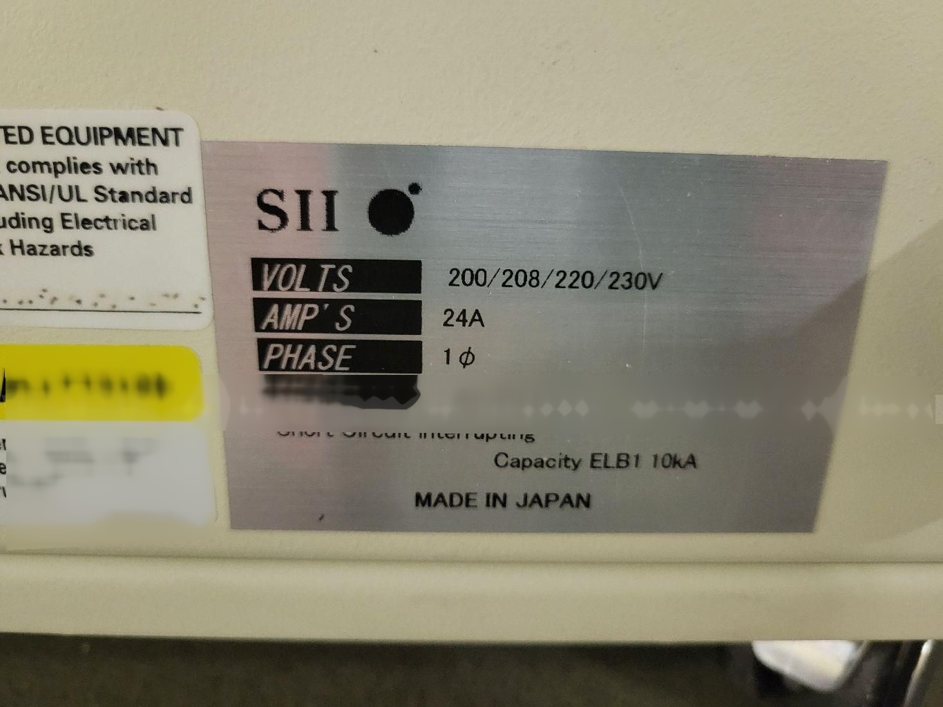
Power Requirement: 200-230V, 50/60HZ
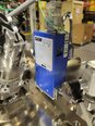
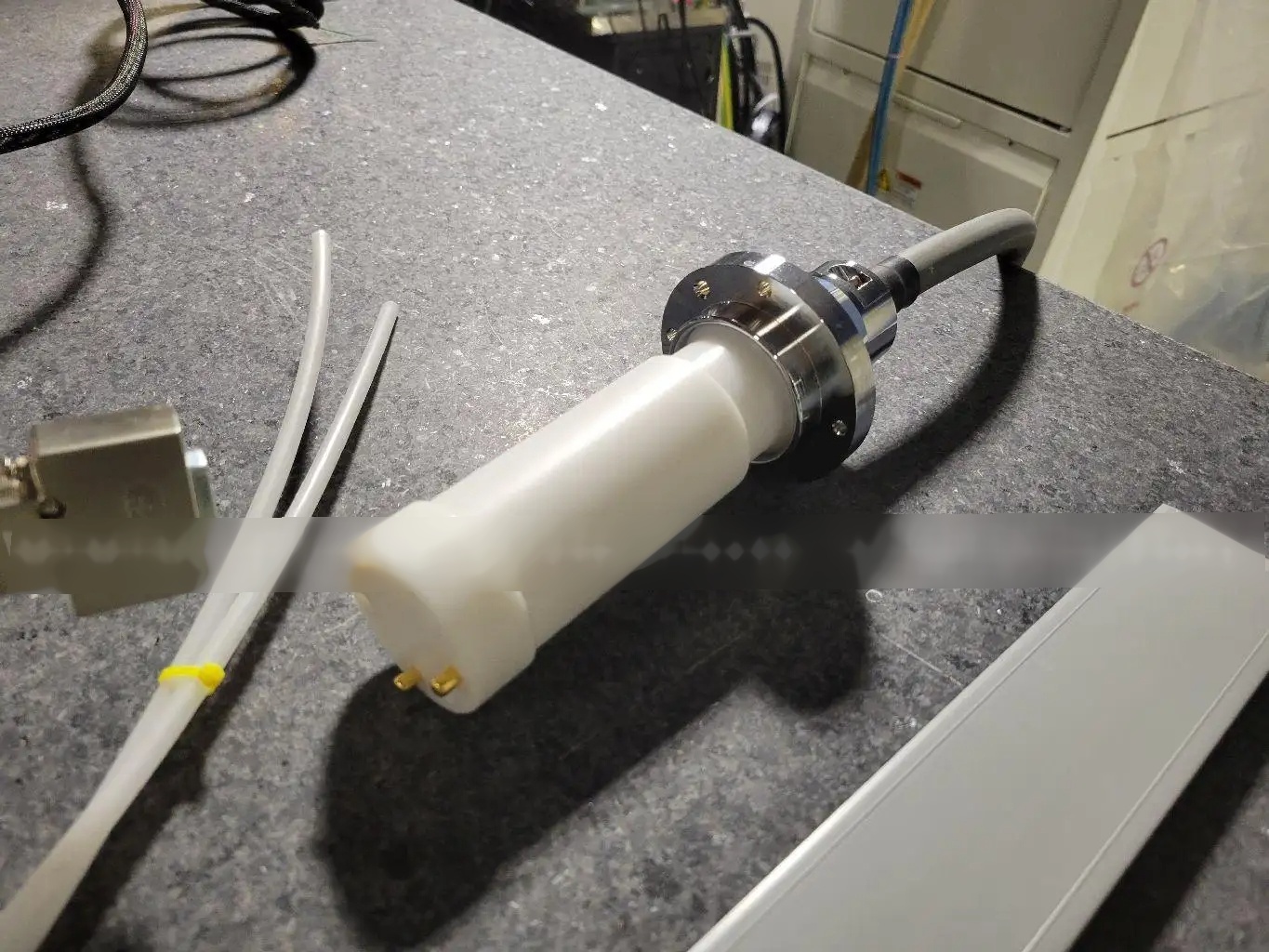
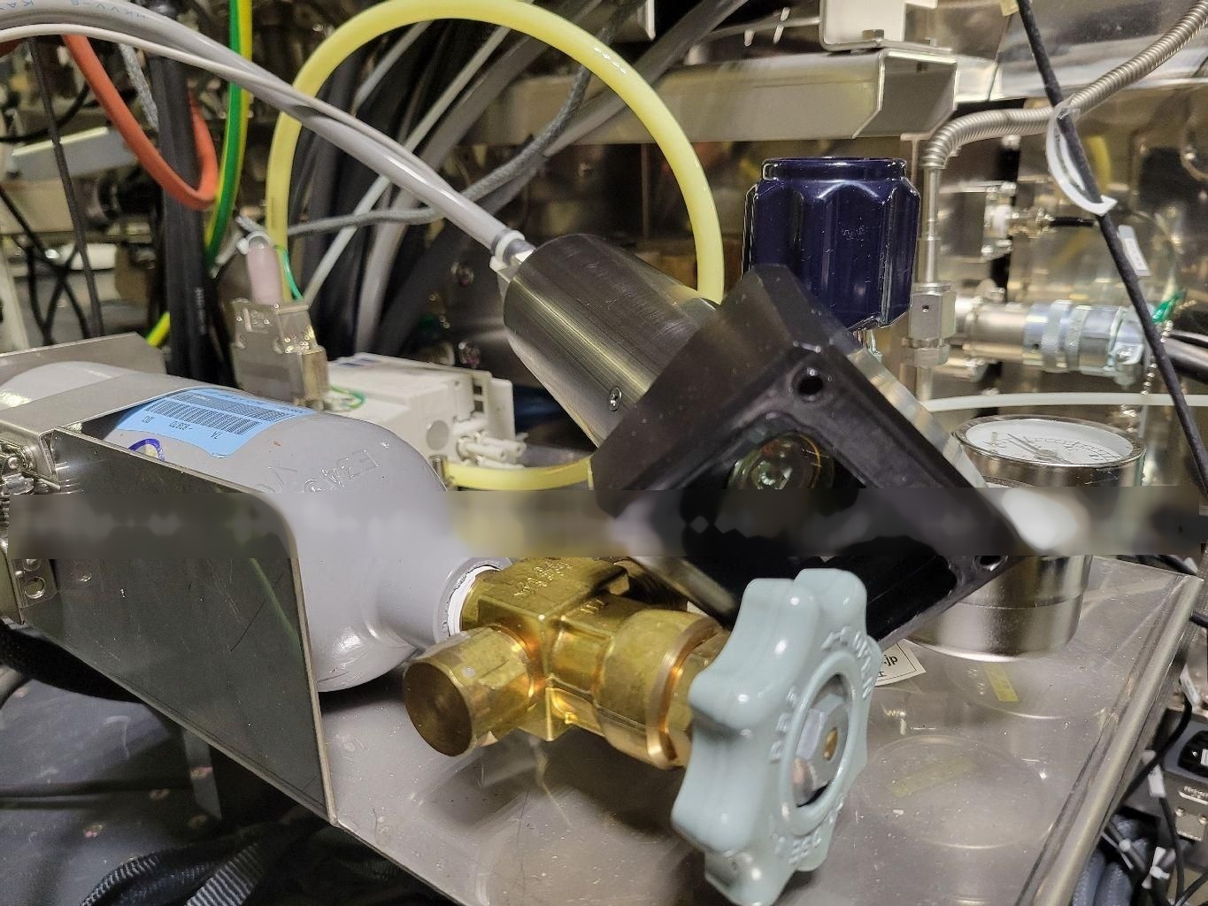
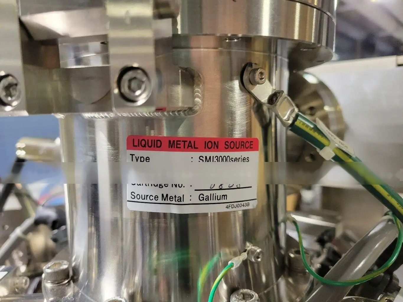
GALLIUM SMI3000 ion source
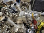
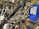
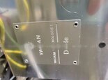
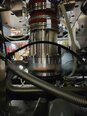
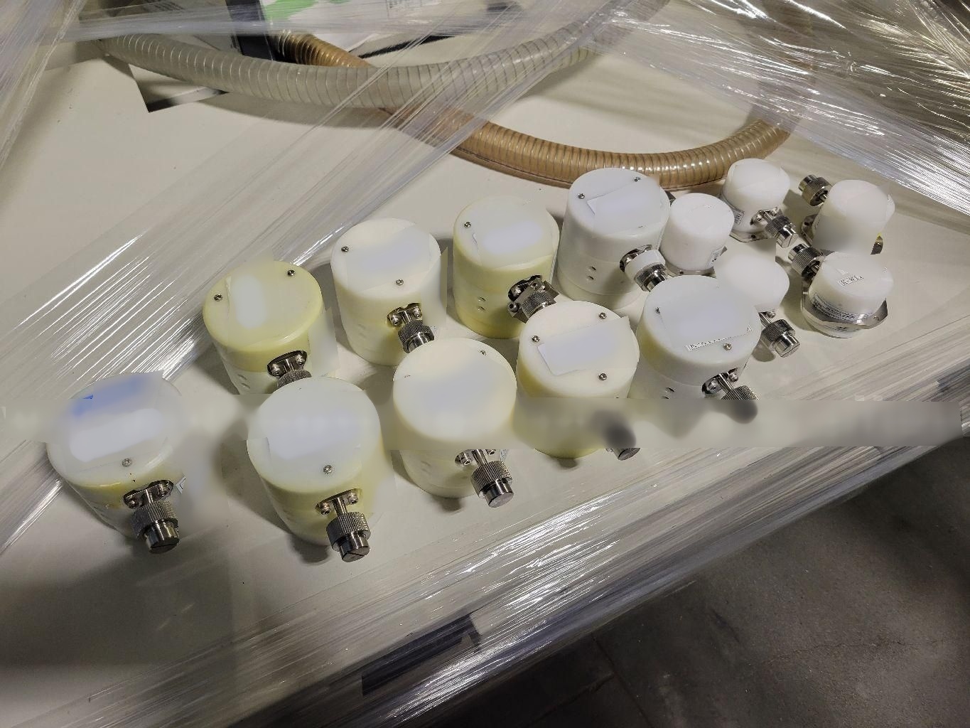
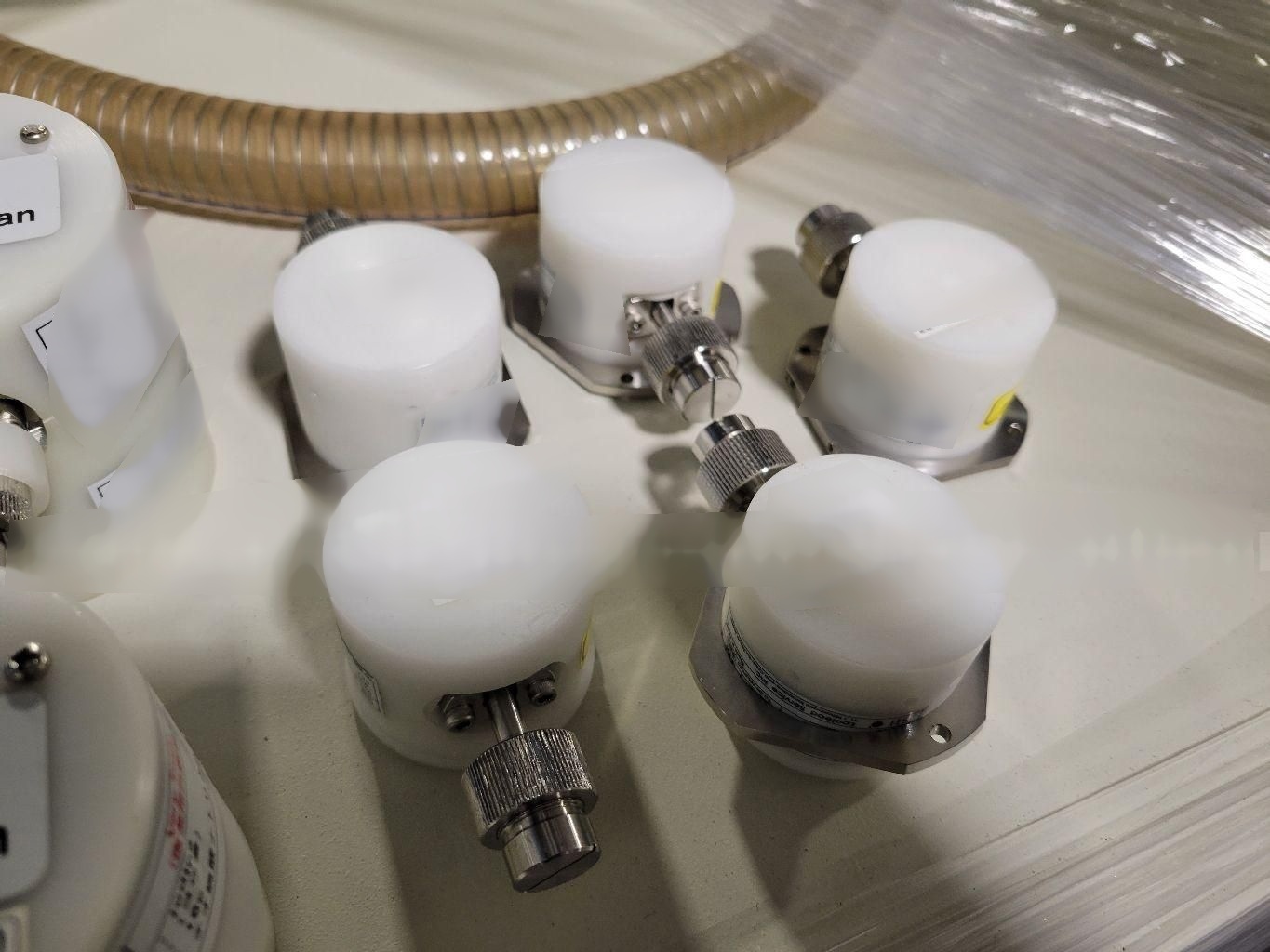
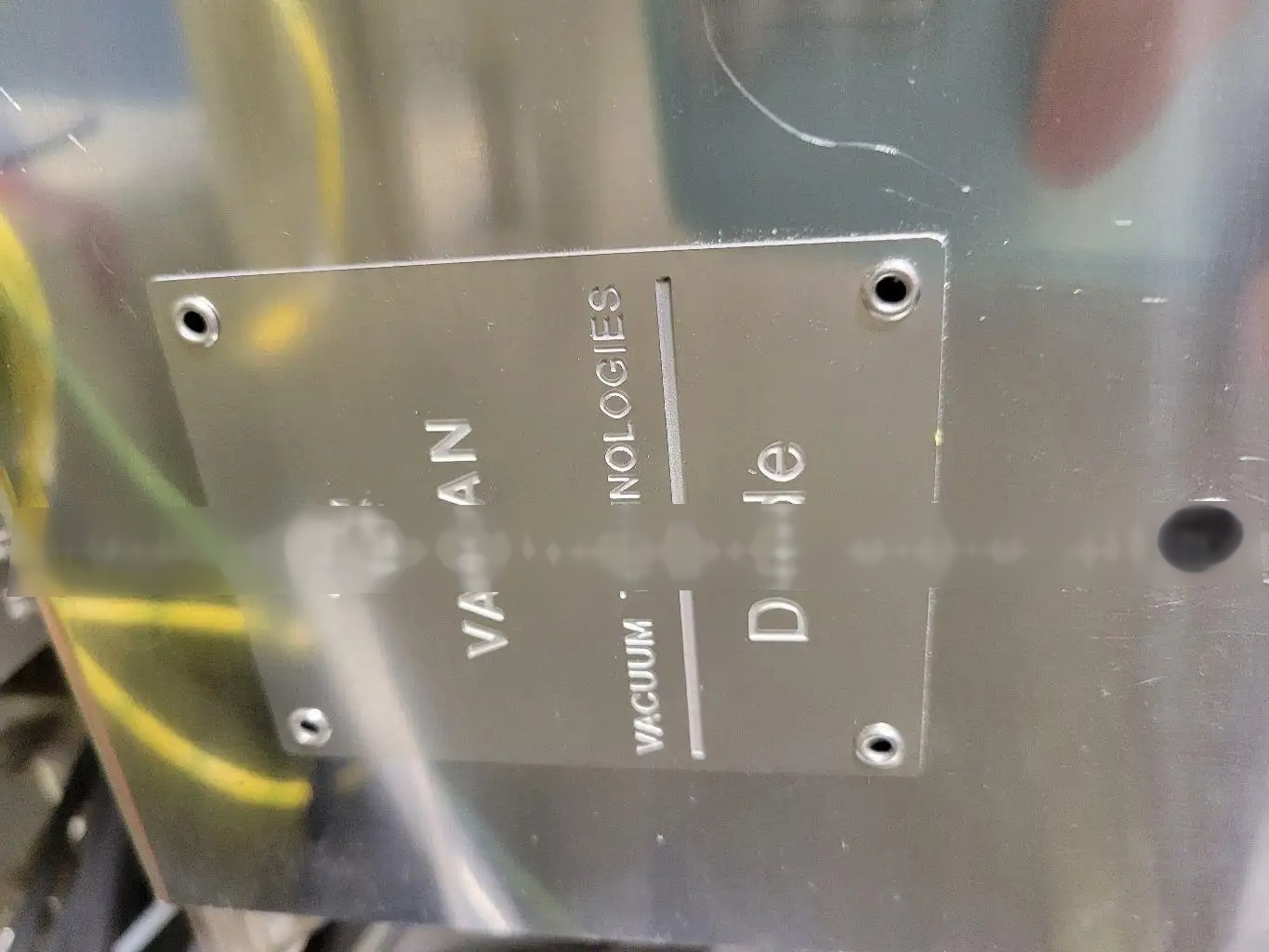
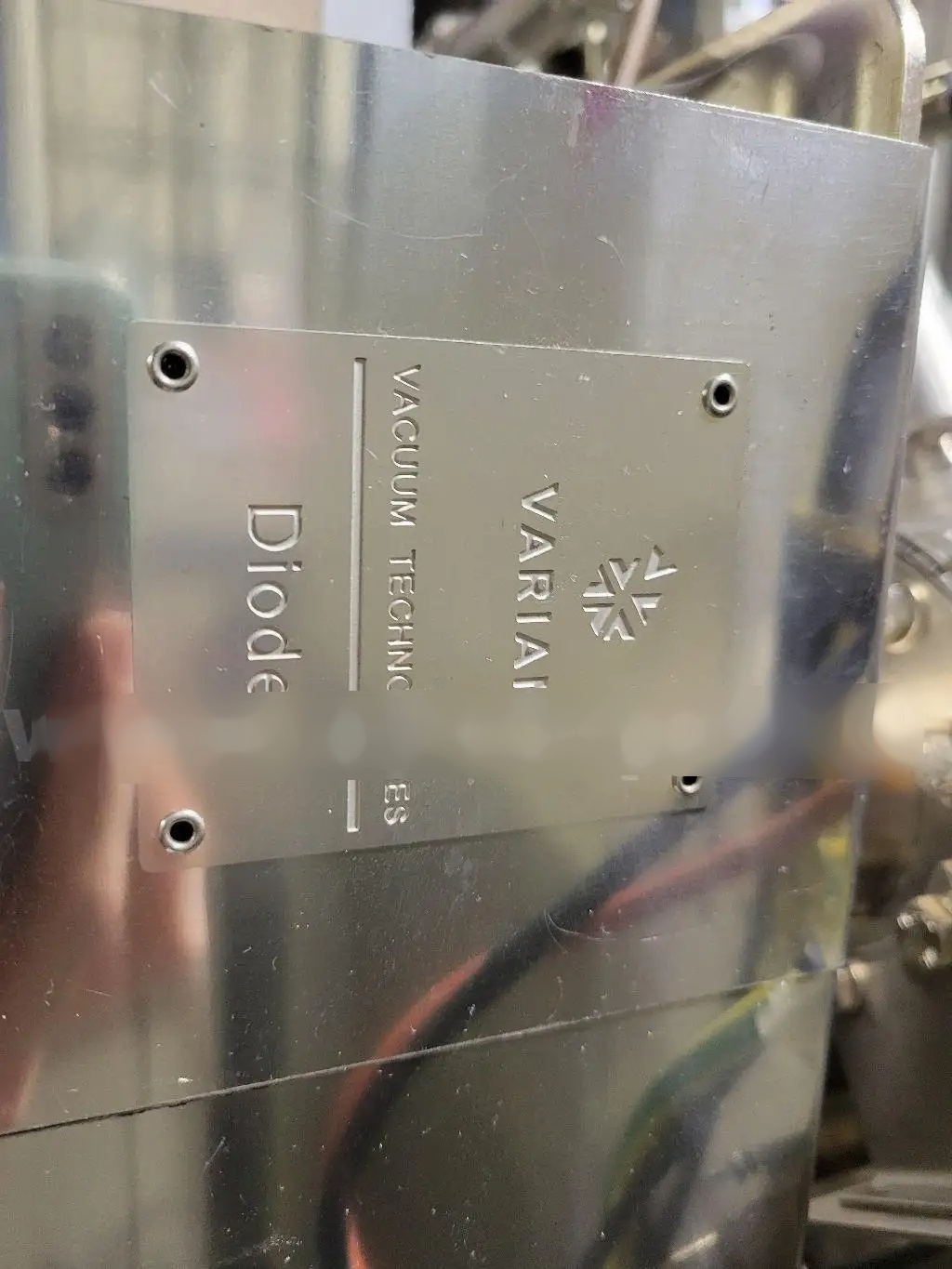
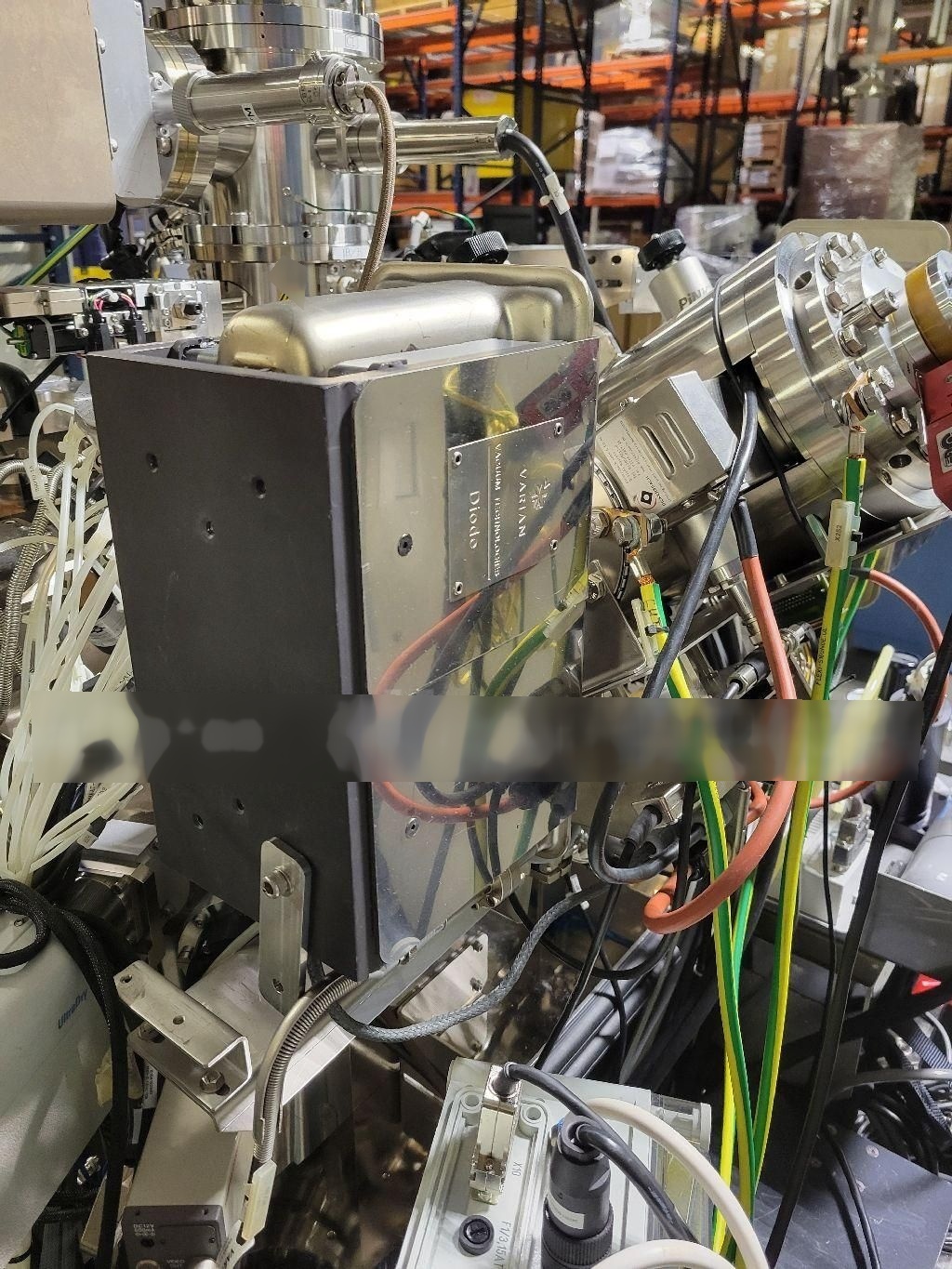
(3) VARIAN Ion pumps
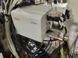
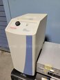
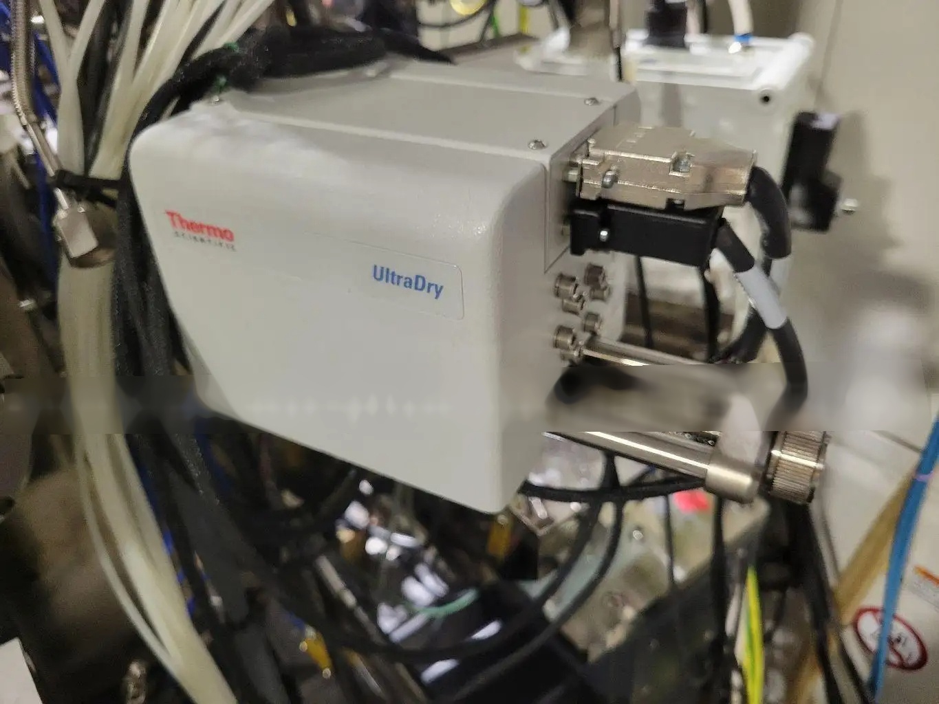
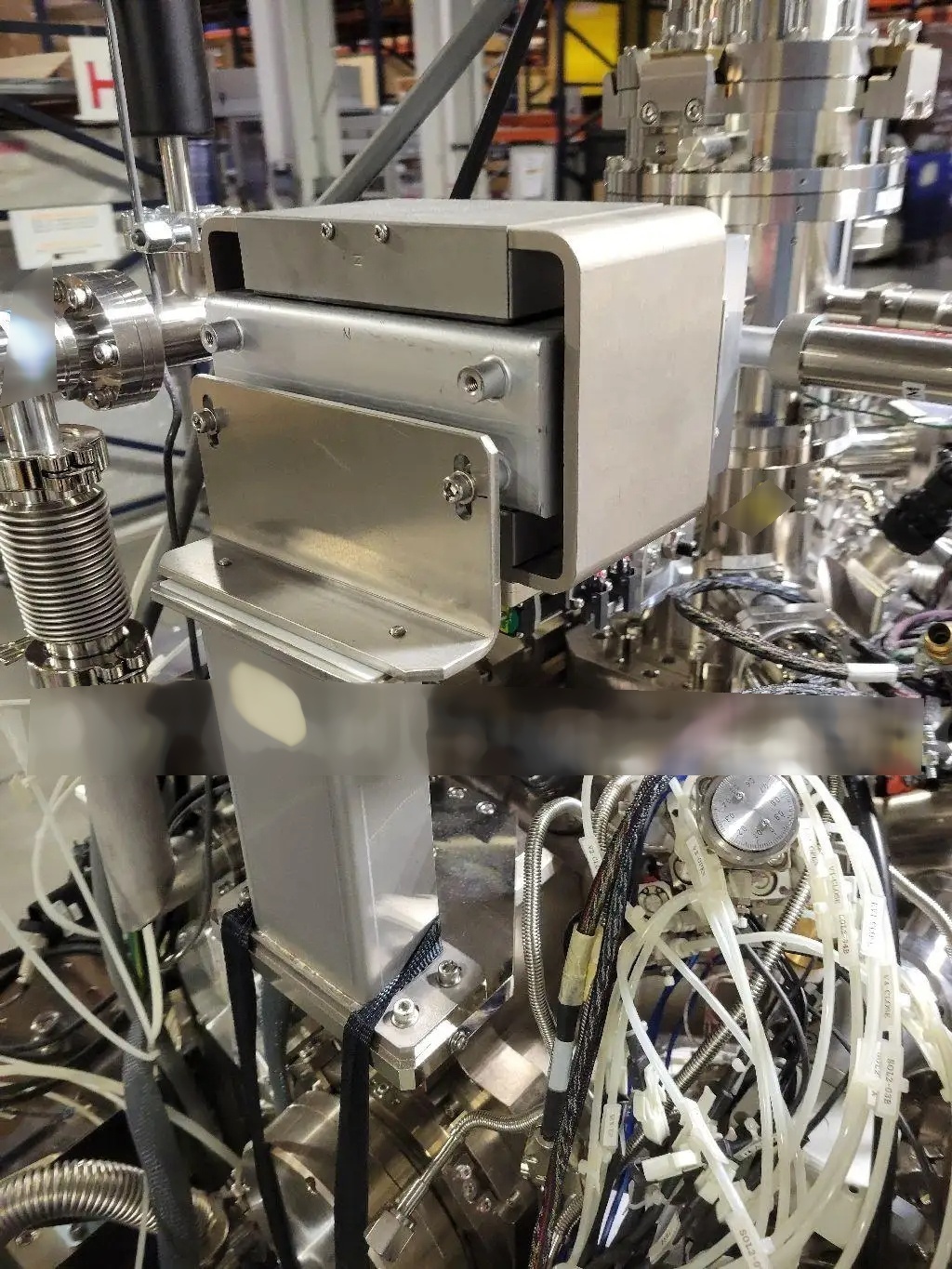
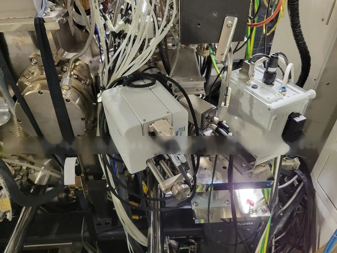
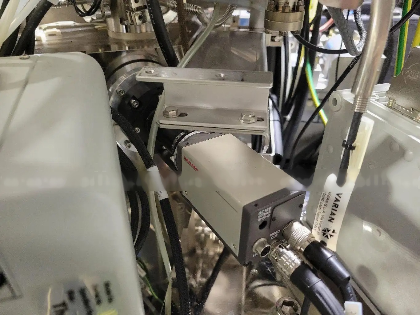
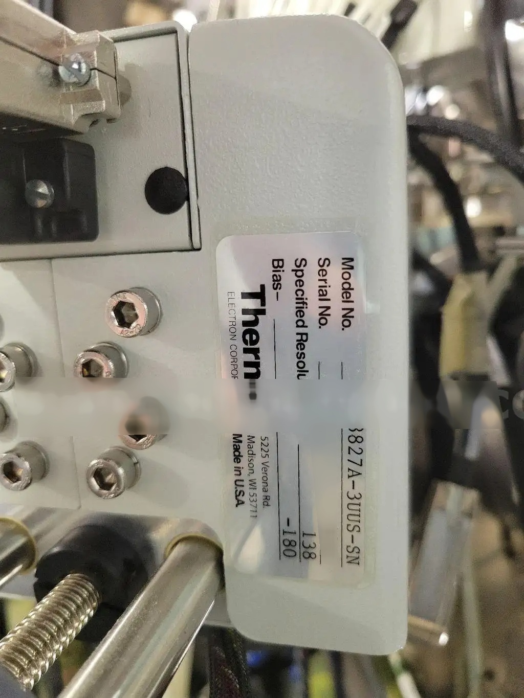
THERMO ELECTRON ULTRADRY Silicon drift detector, P/N: 8827A-3UUS-SN
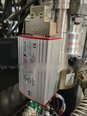
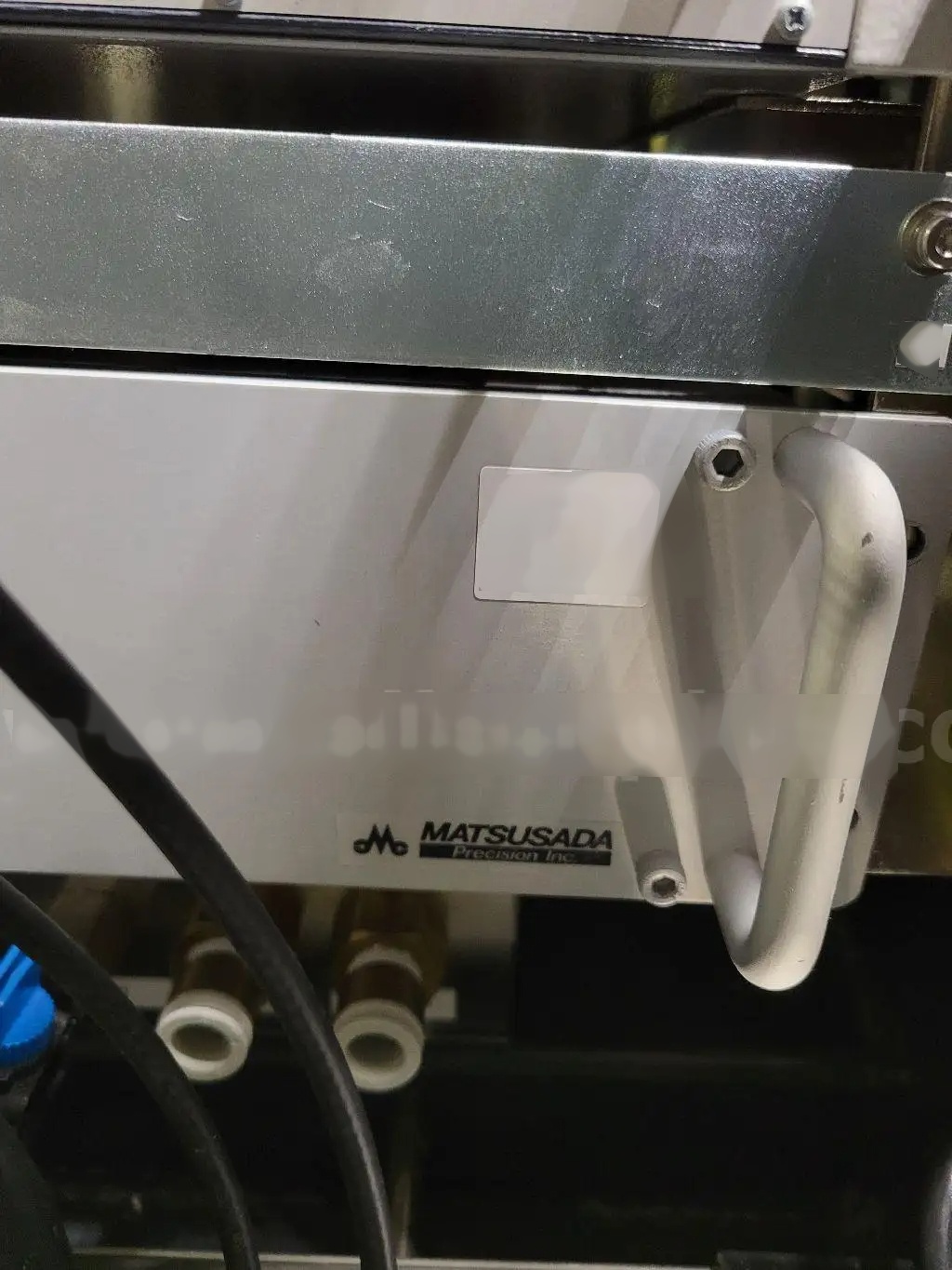
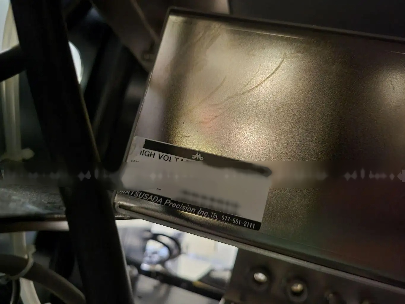
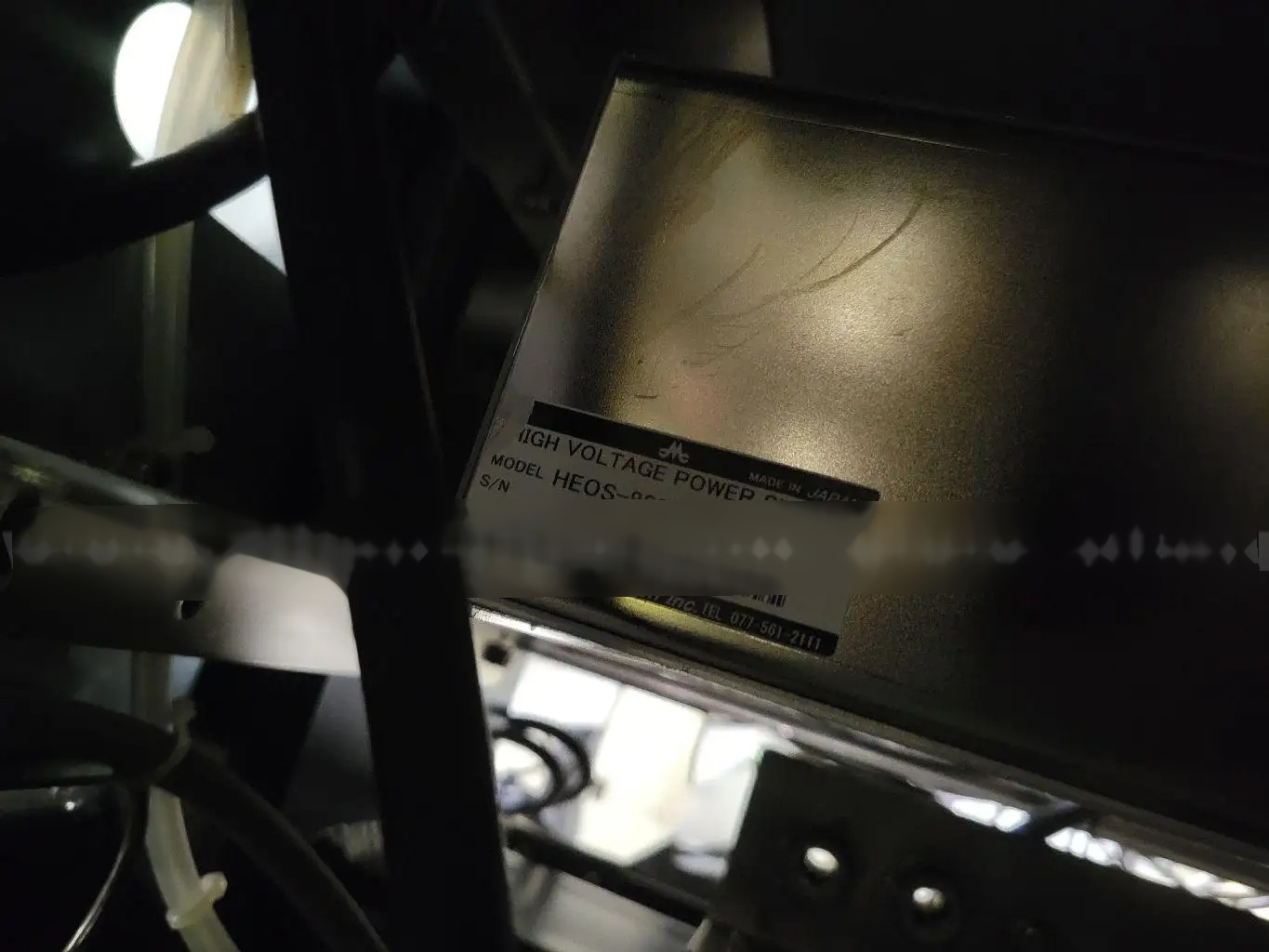
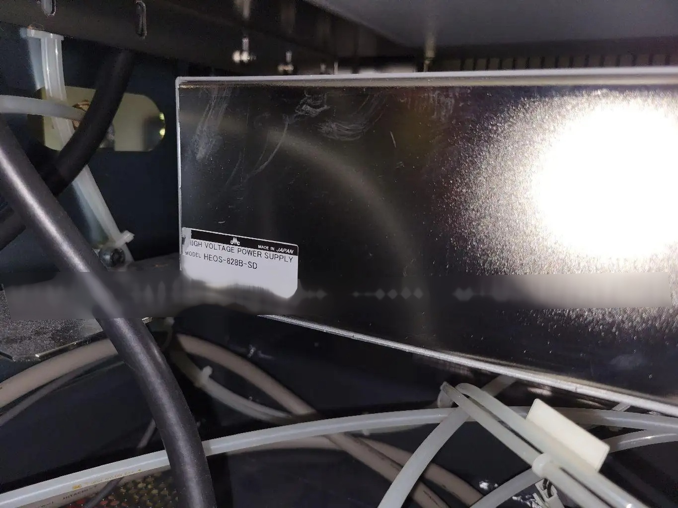
MATSUSADA HEOS-828B-SD HV Power supply
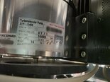
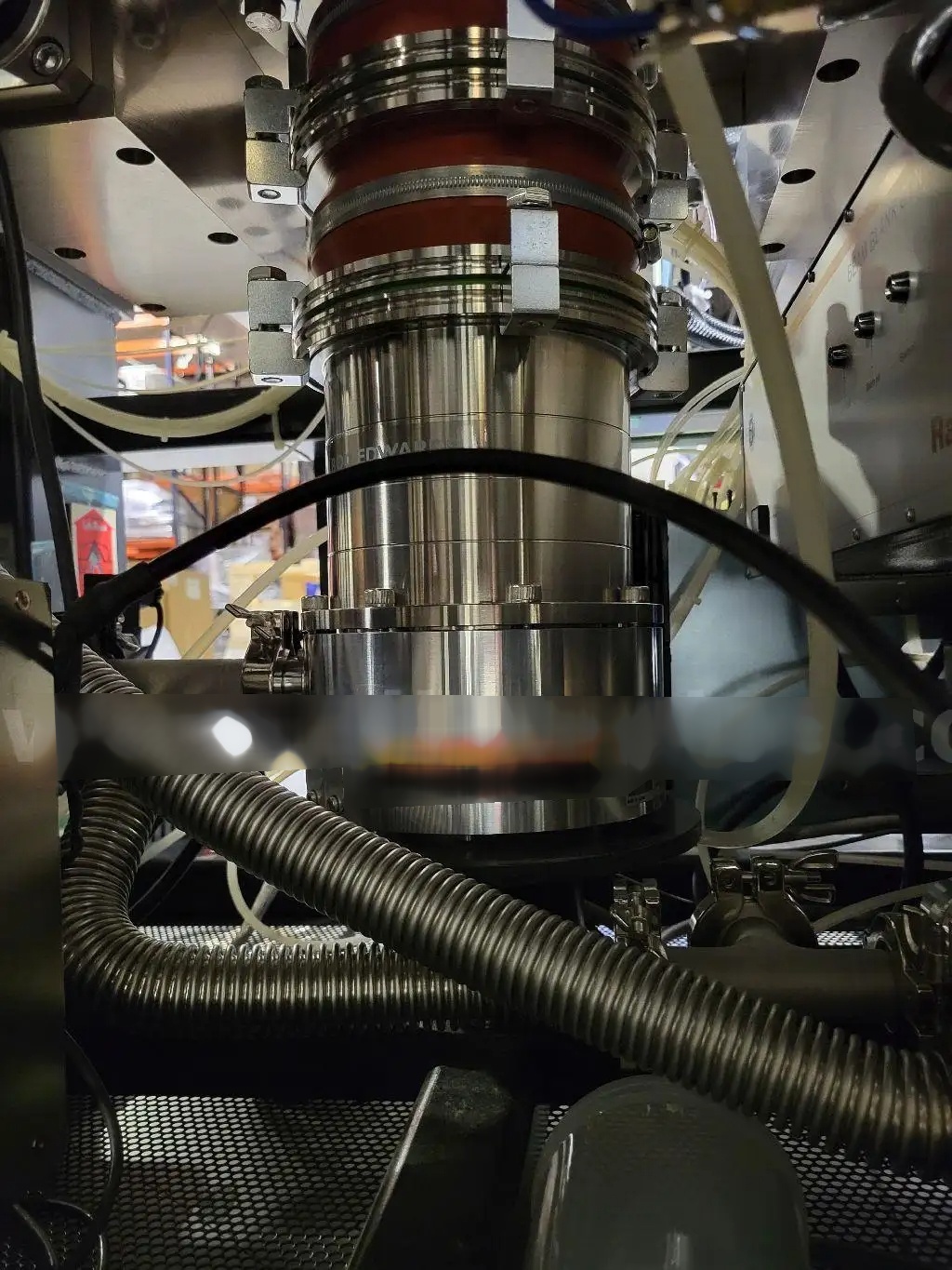
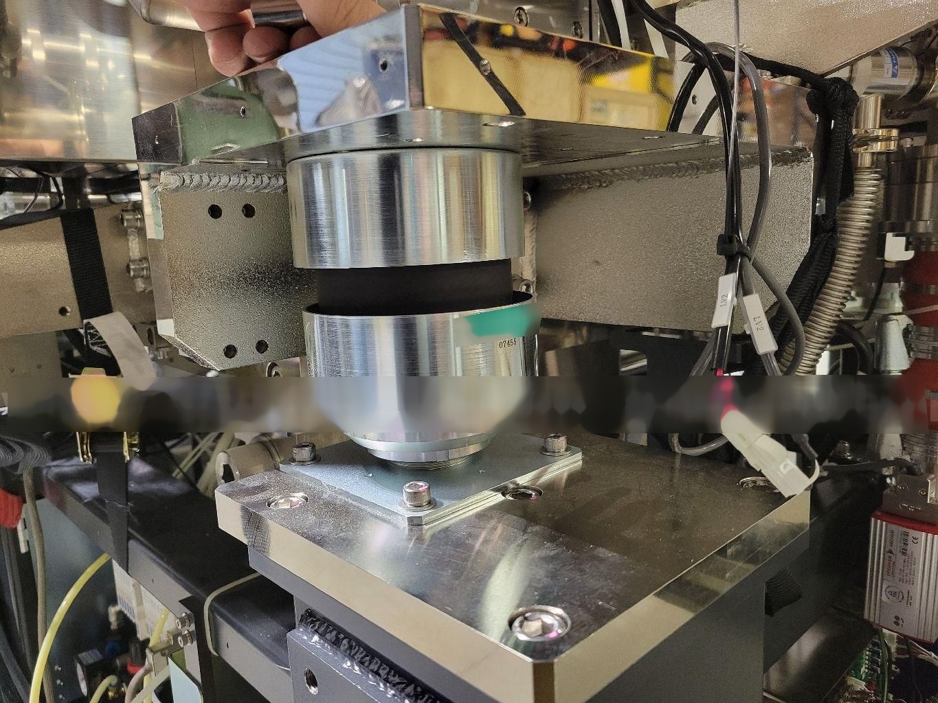
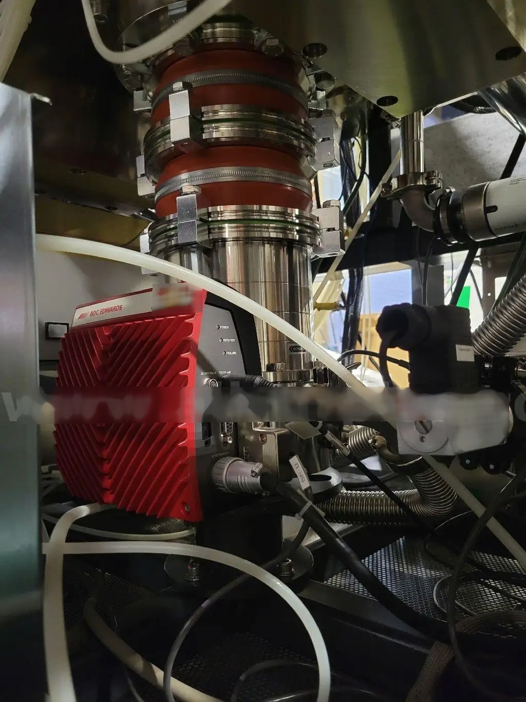
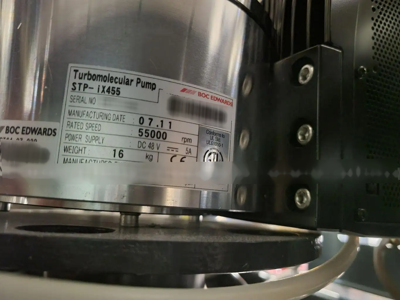
BOC EDWARDS STP-iX455 Chamber turbopump
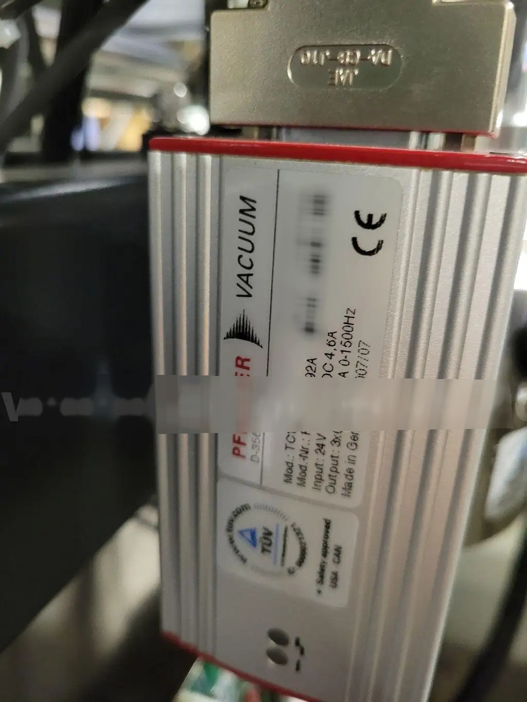
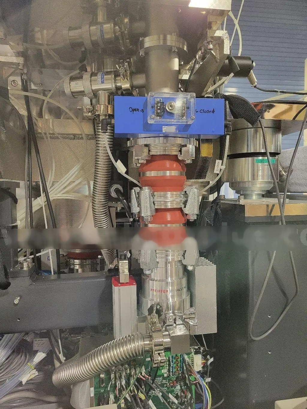
PFEIFFER Loadlock turbopump
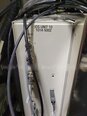
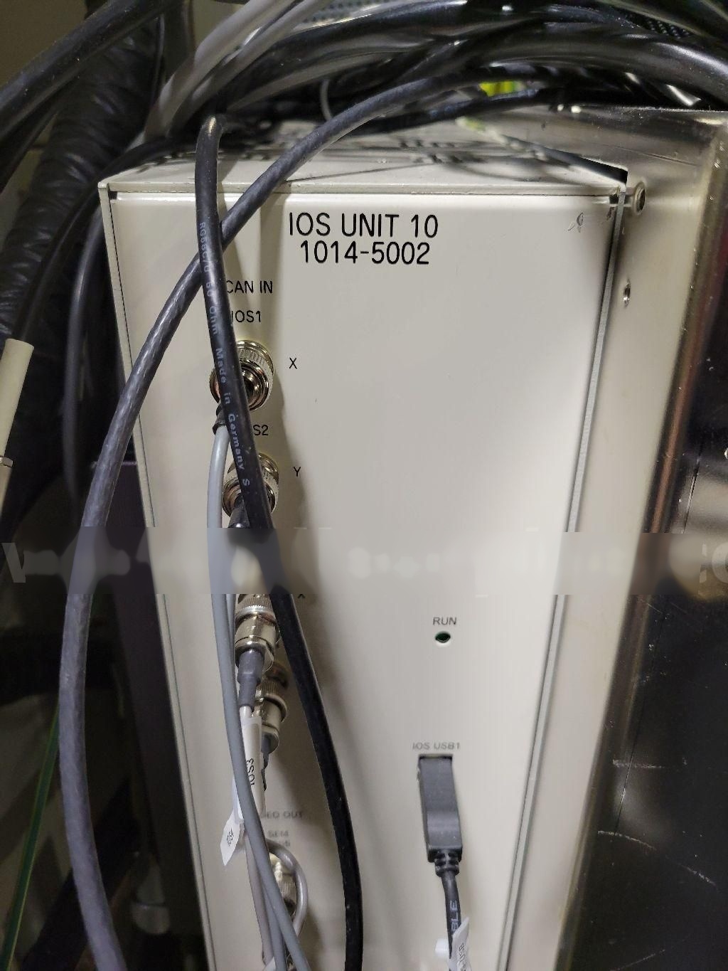
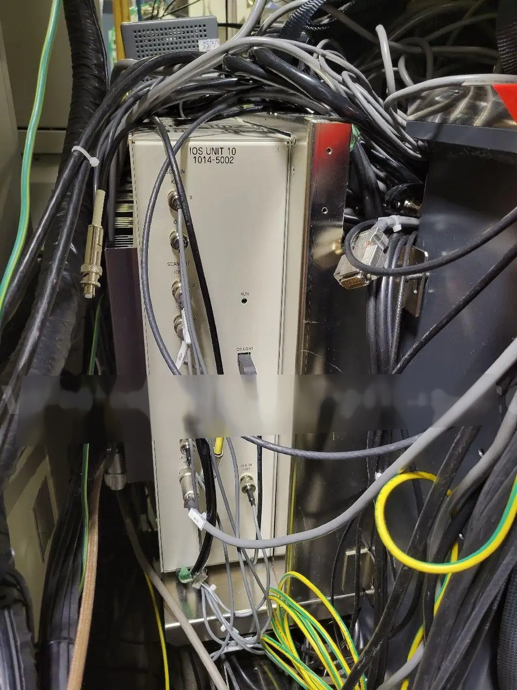
IOS Unit, P/N: 1014-5002
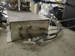
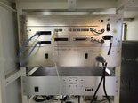
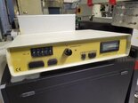
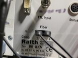
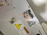
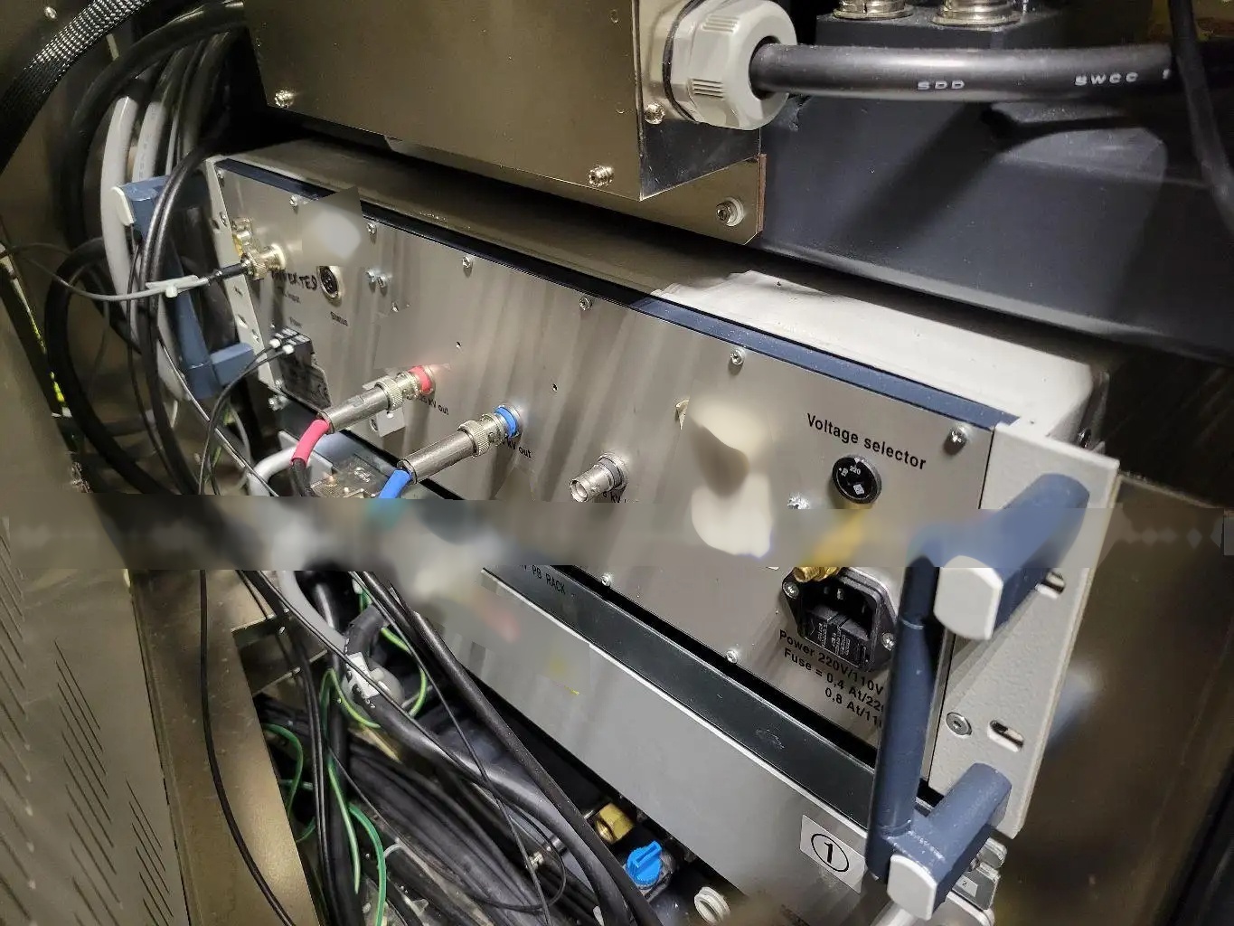
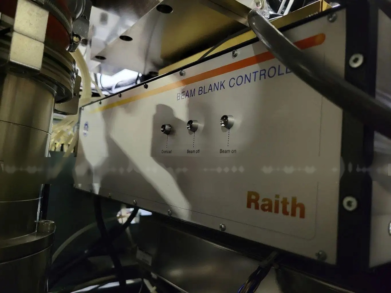
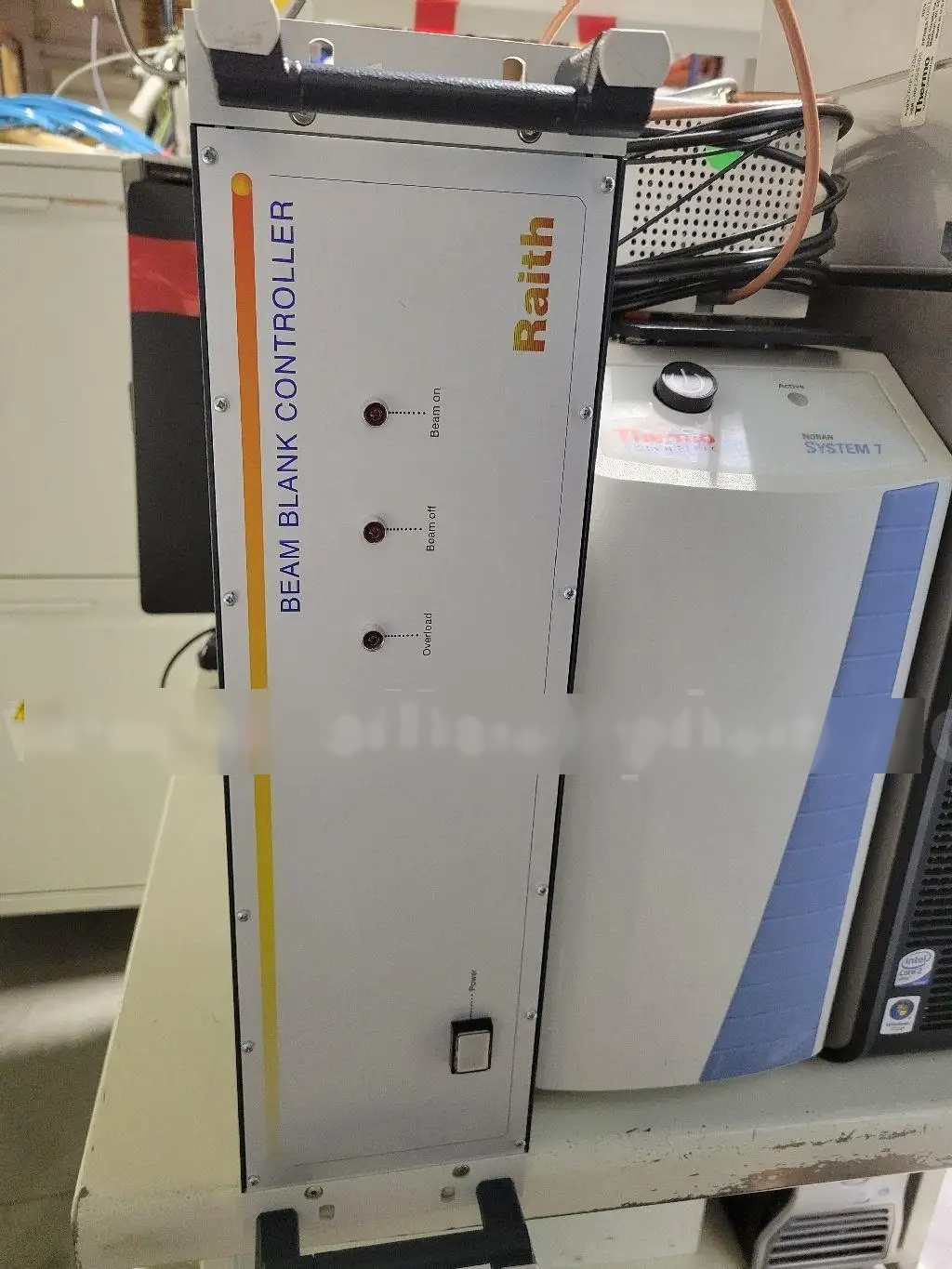
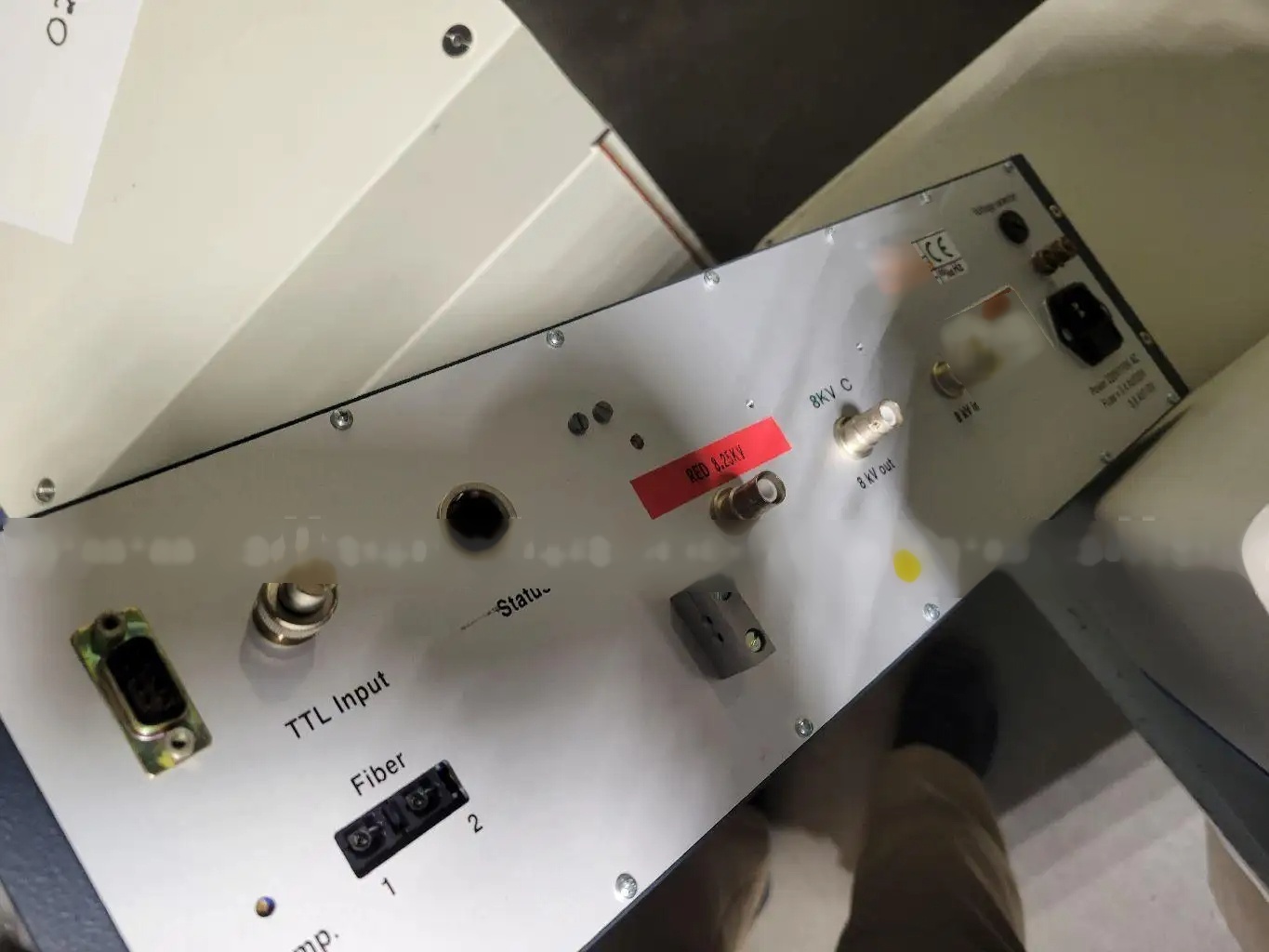
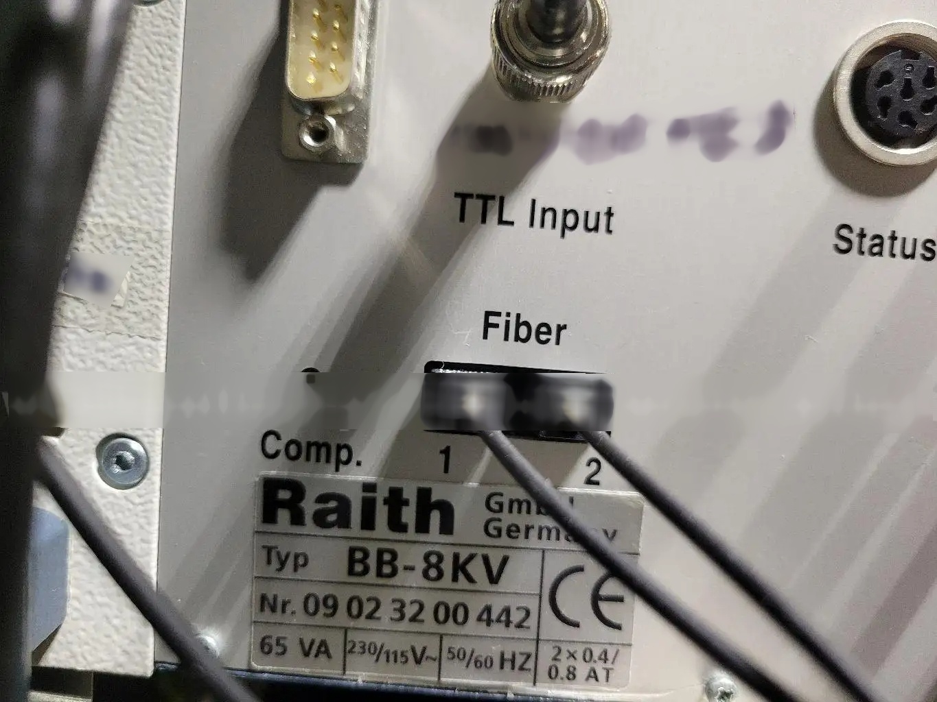
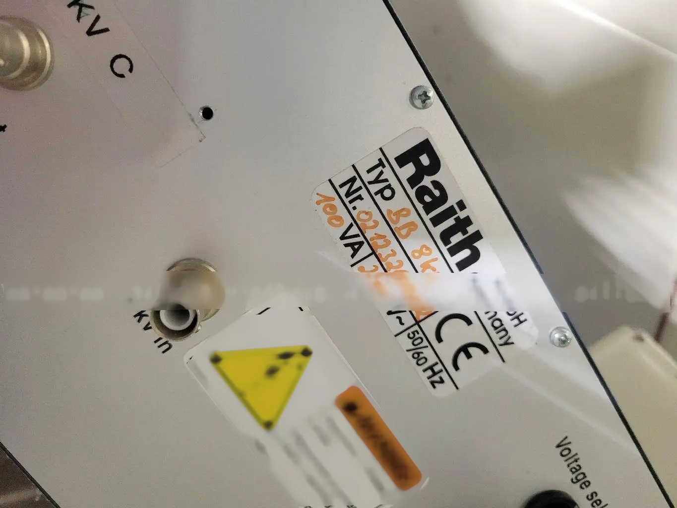
RAITH BB-8KV Beam blank controller
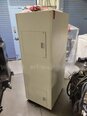
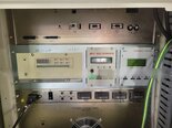
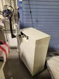
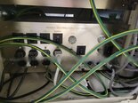
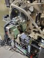
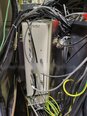
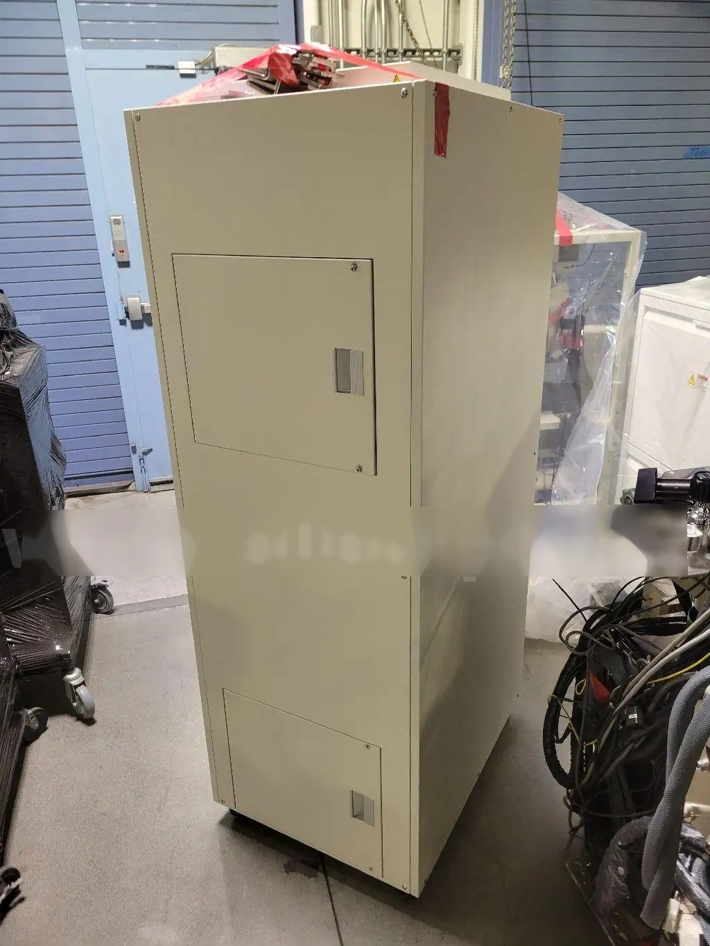
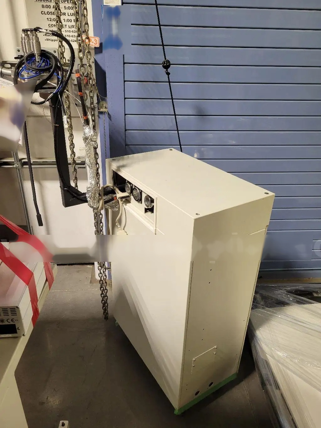
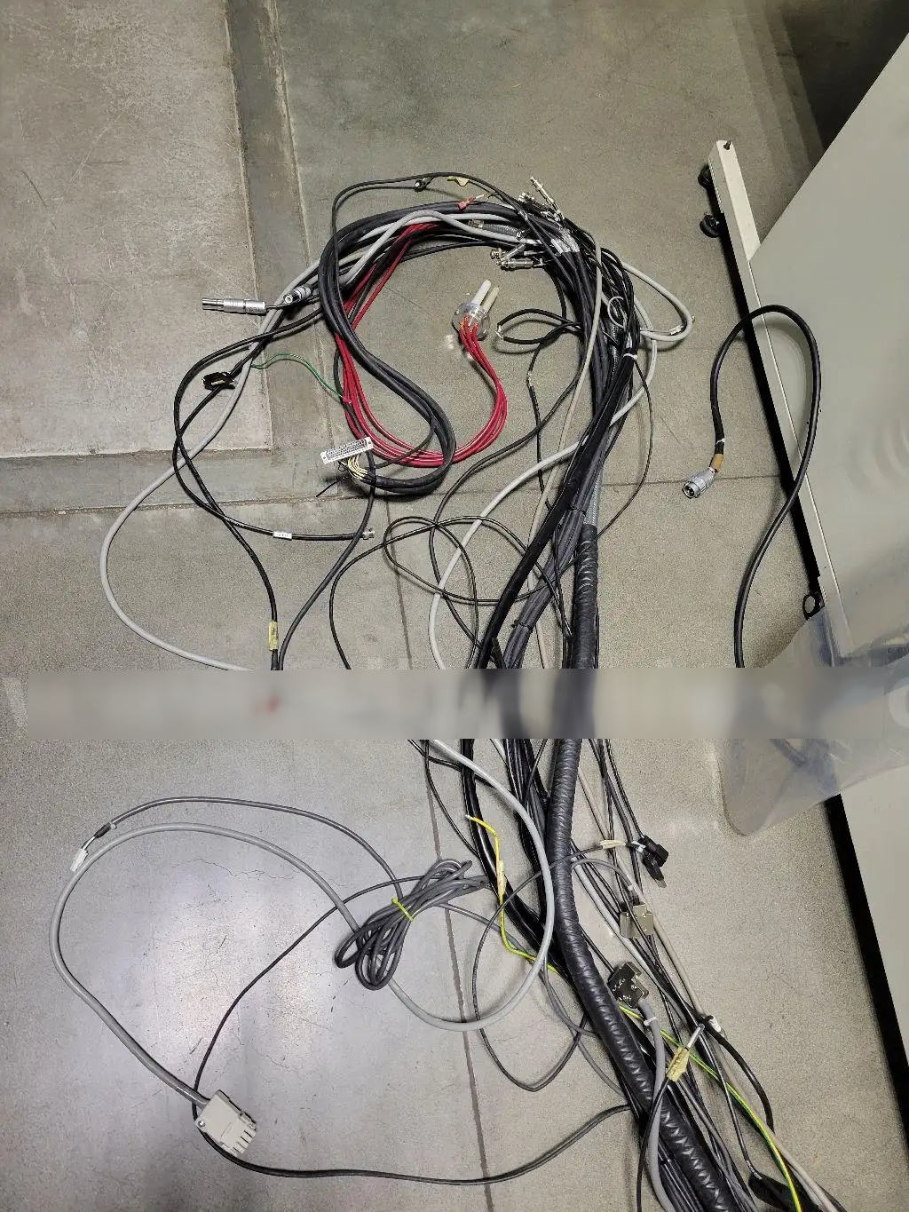
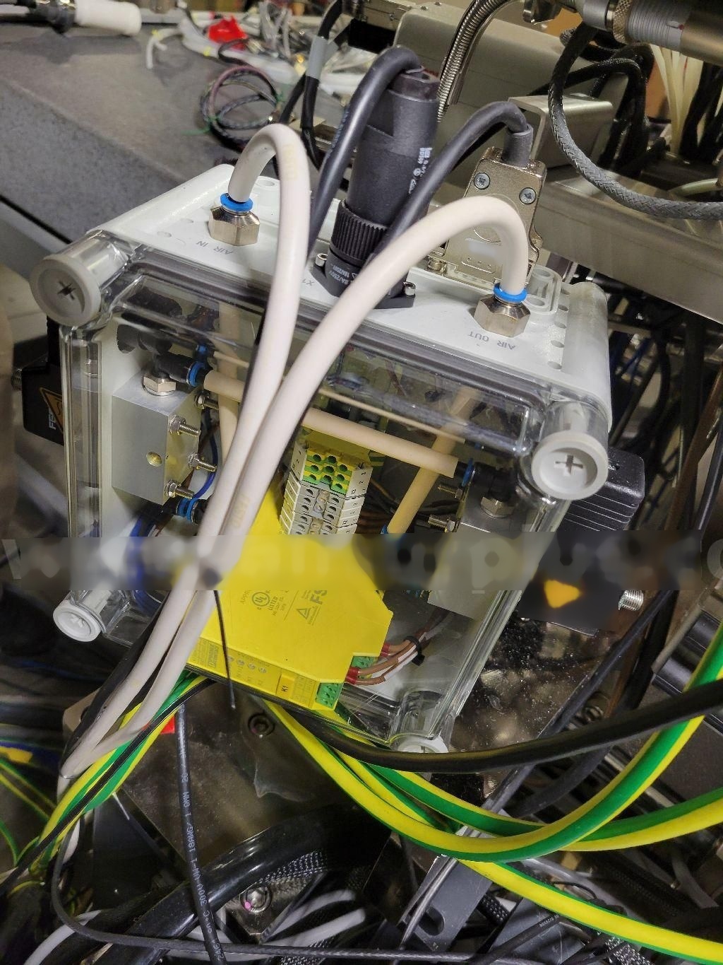
Control cabinet
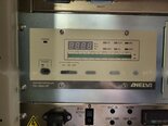
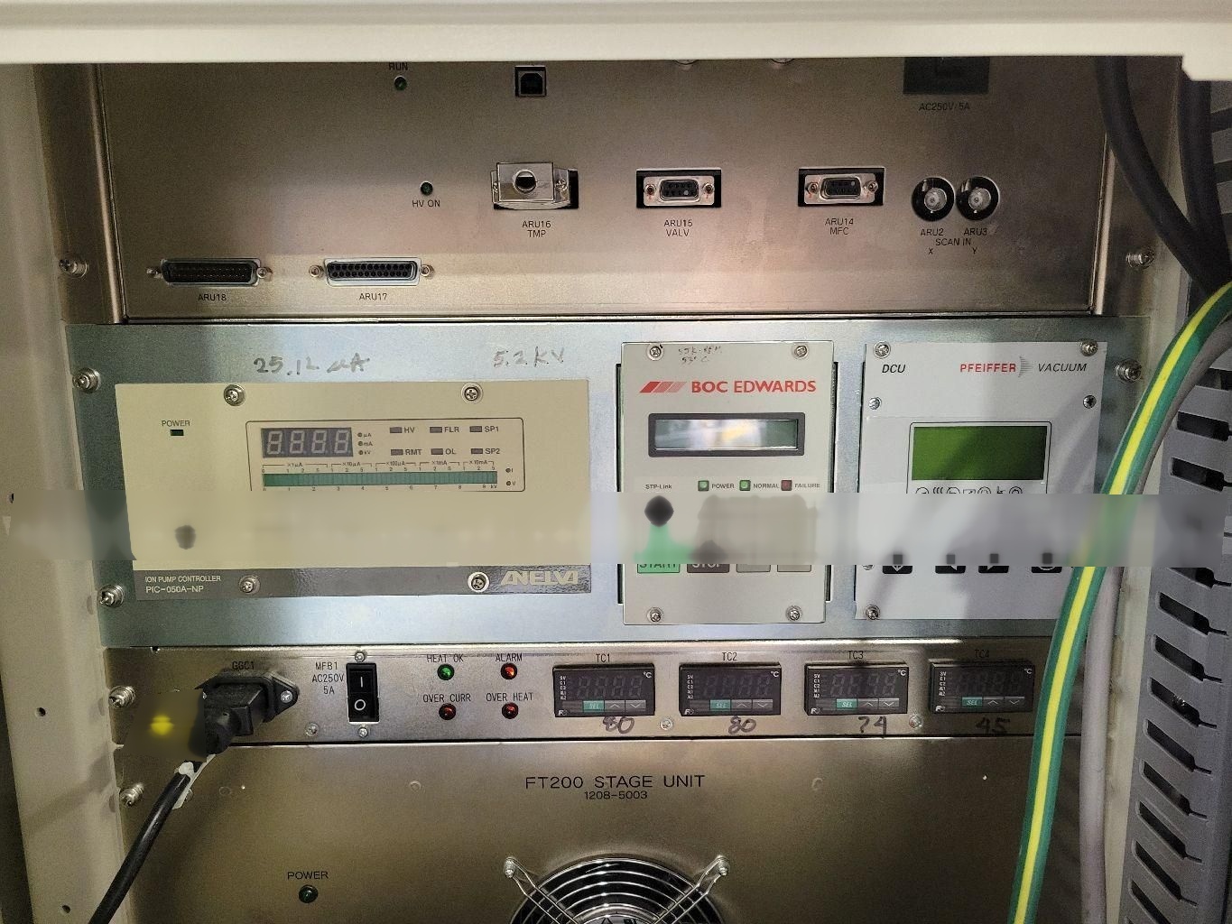
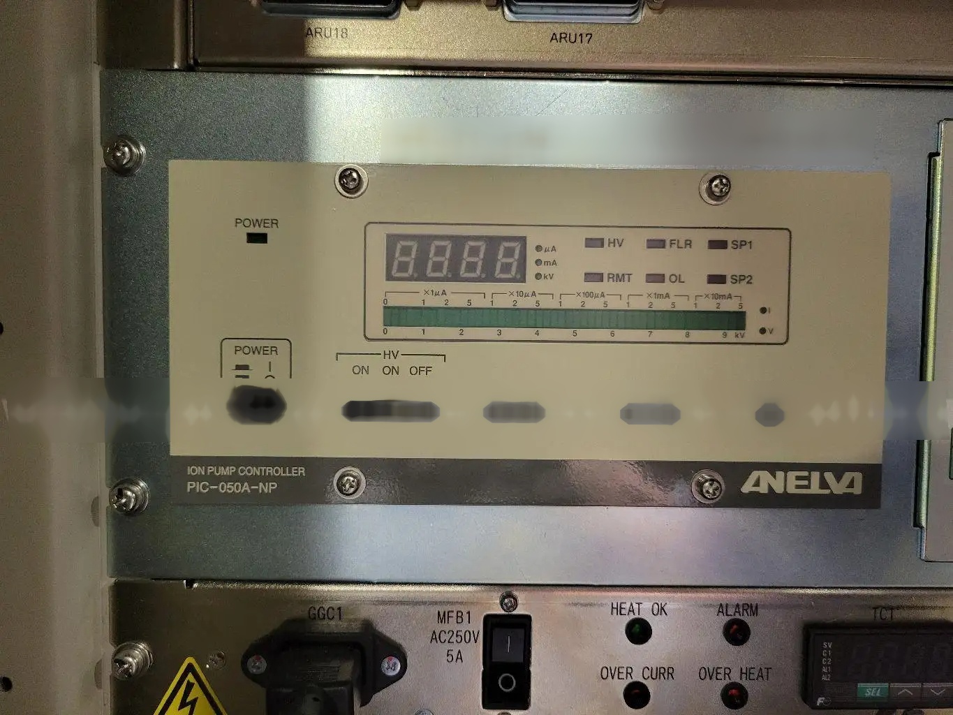
ANELVA PIC-050A-NP Ion pump controller
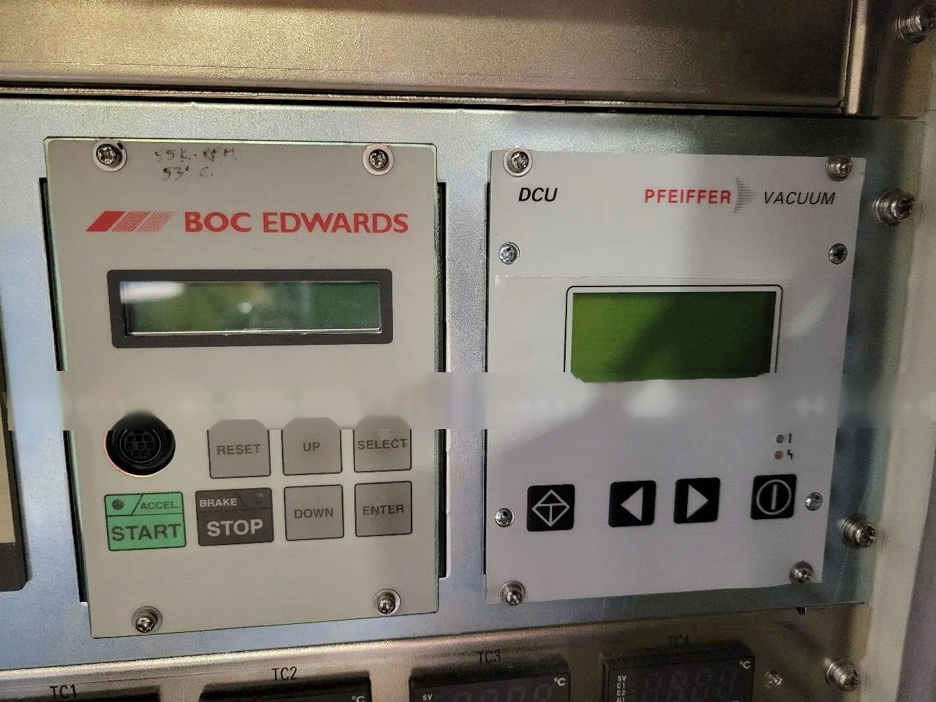
BOC EDWARDS Pump controller
PFEIFFER DCU Pump controller
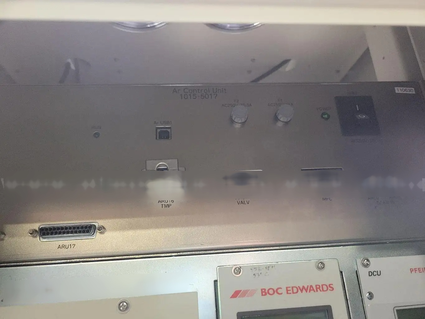
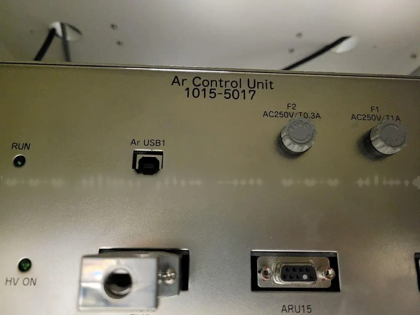
Ar control unit, P/N: 1015-5017
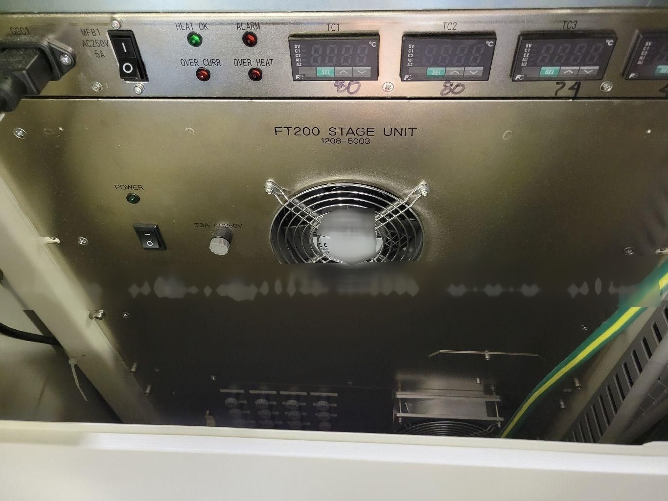
FT200 Stage controller, P/N: 1208-5003
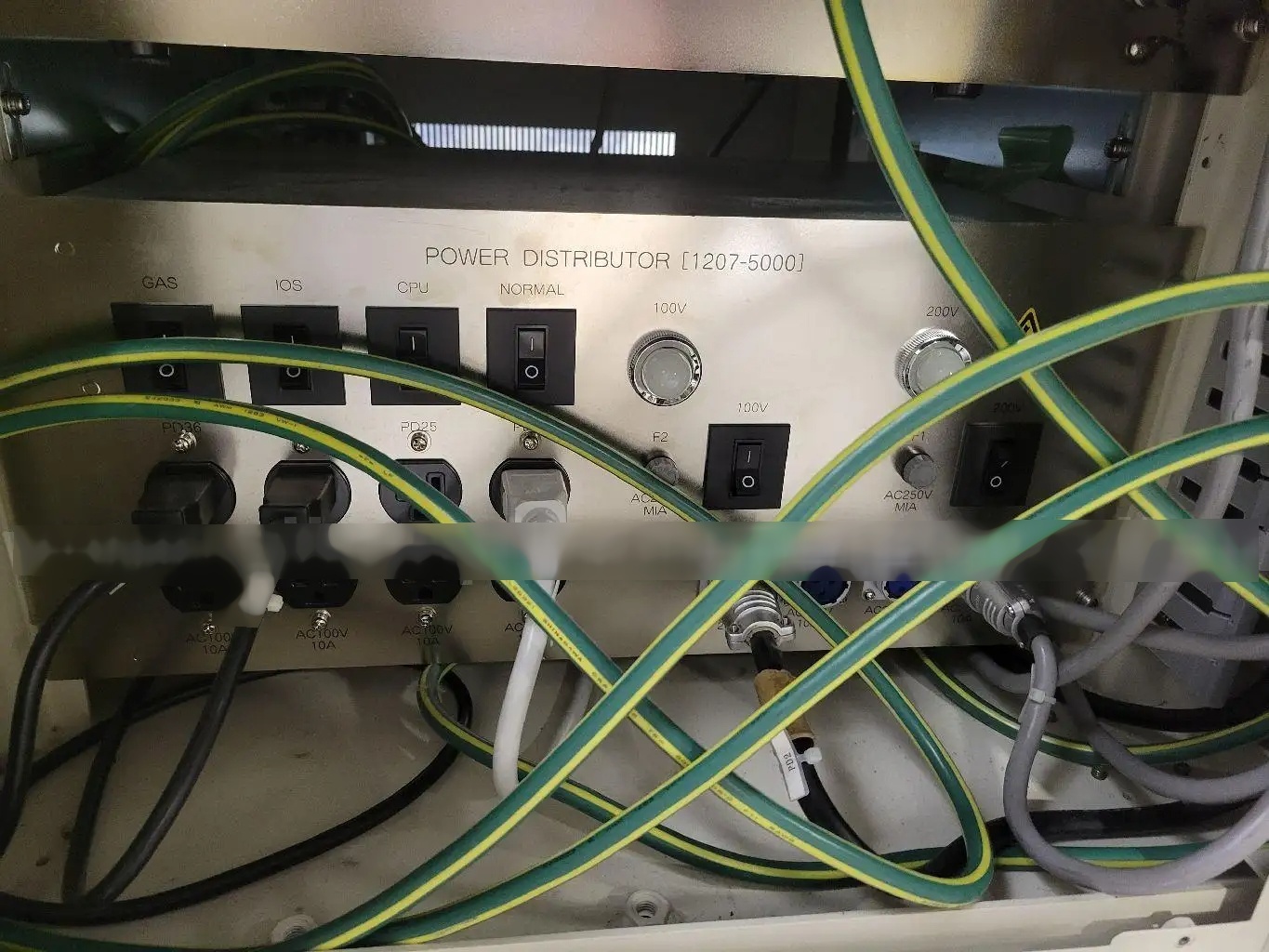
PDU, P/N: 1207-5000
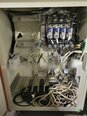
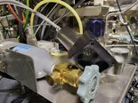
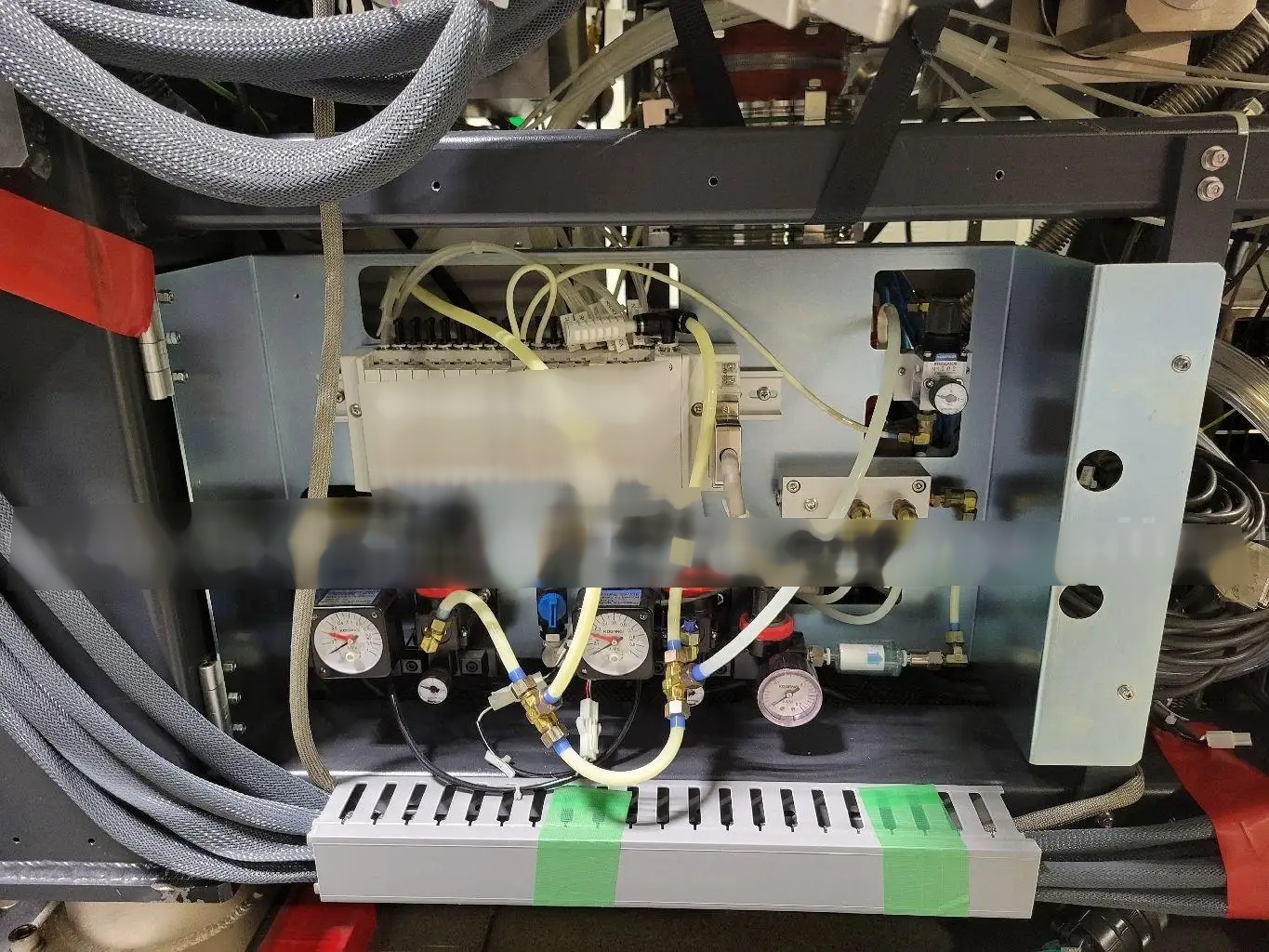
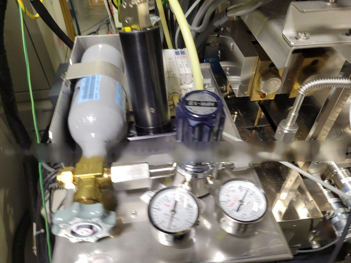
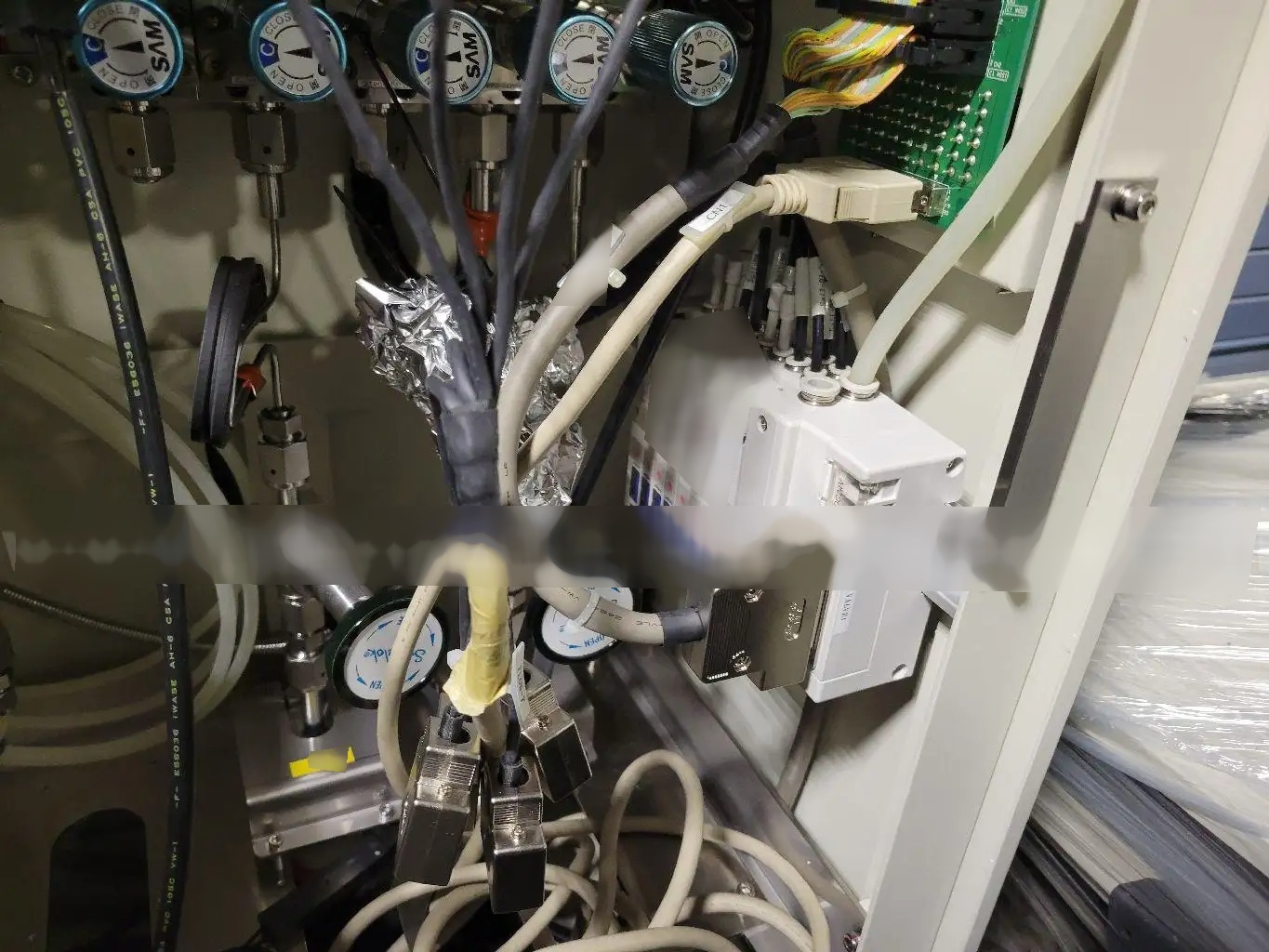
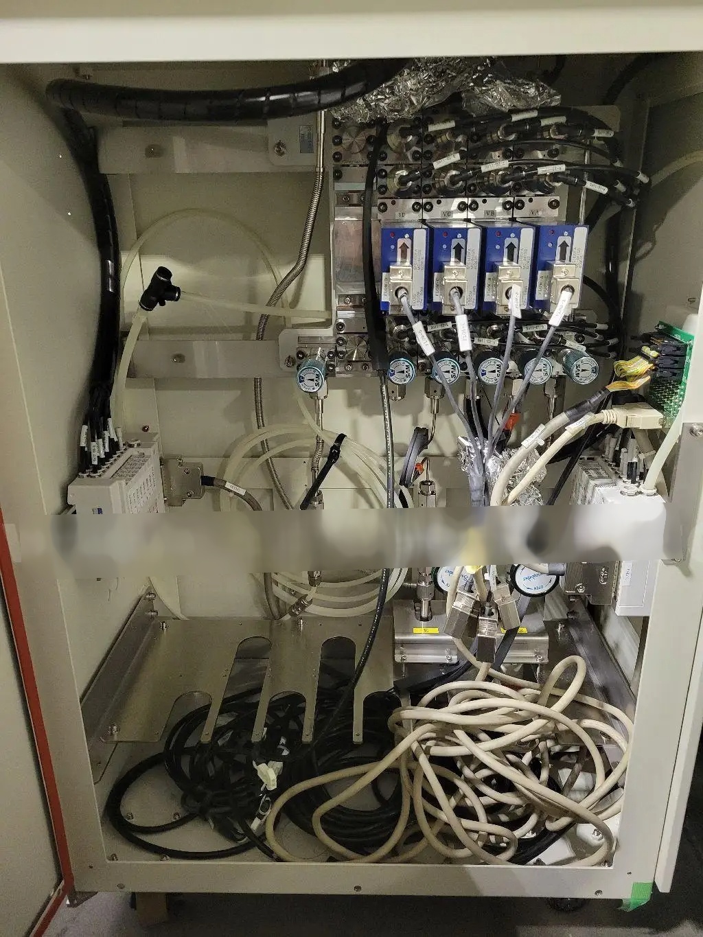
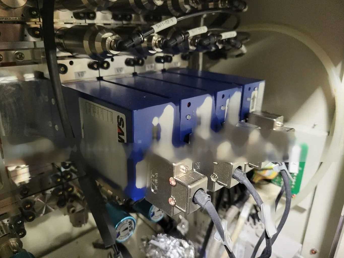
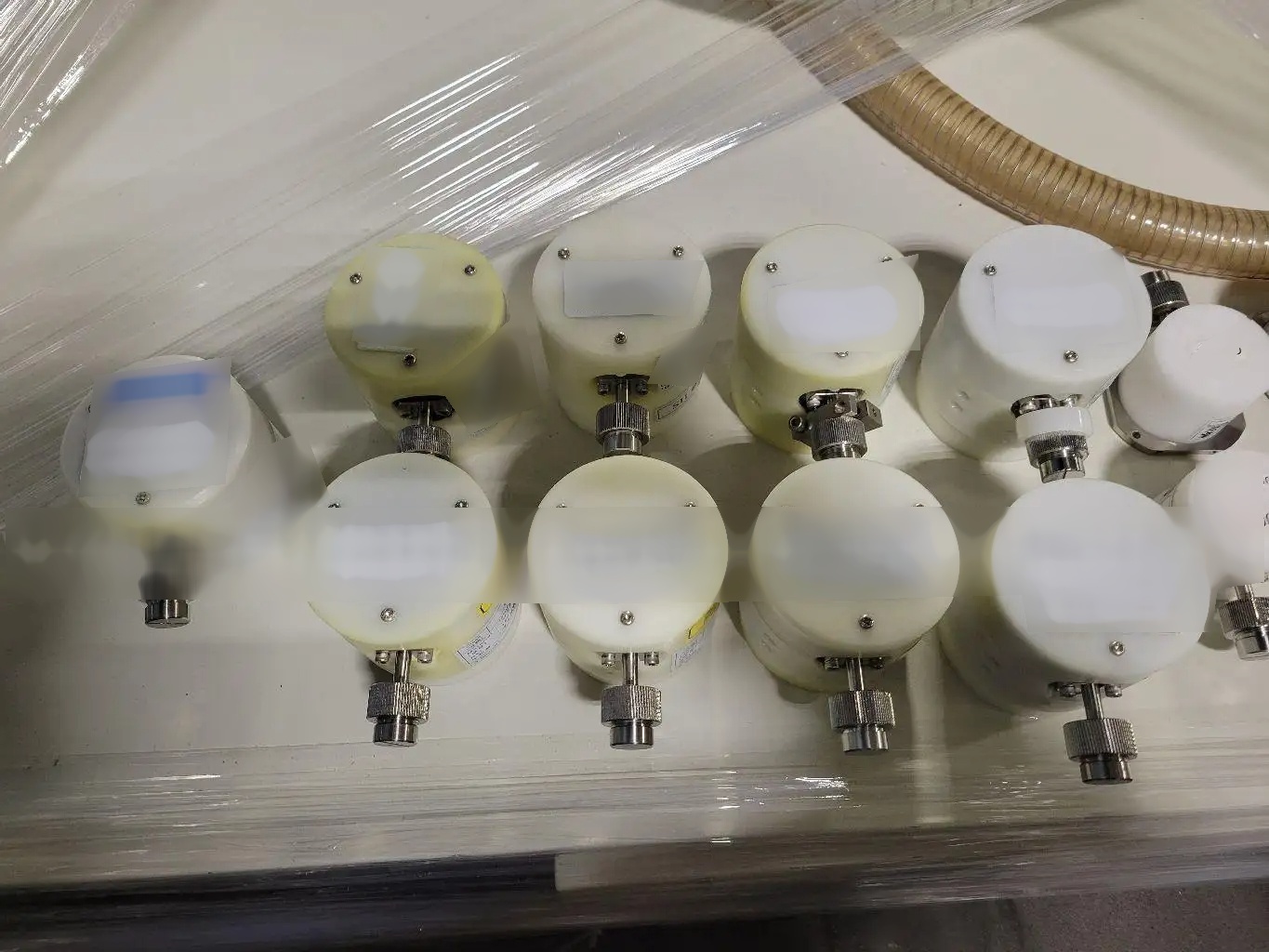
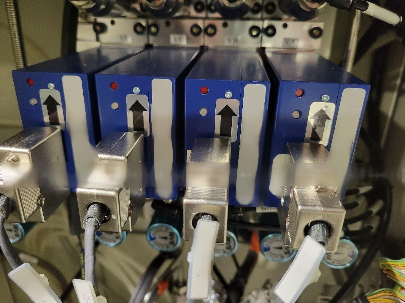
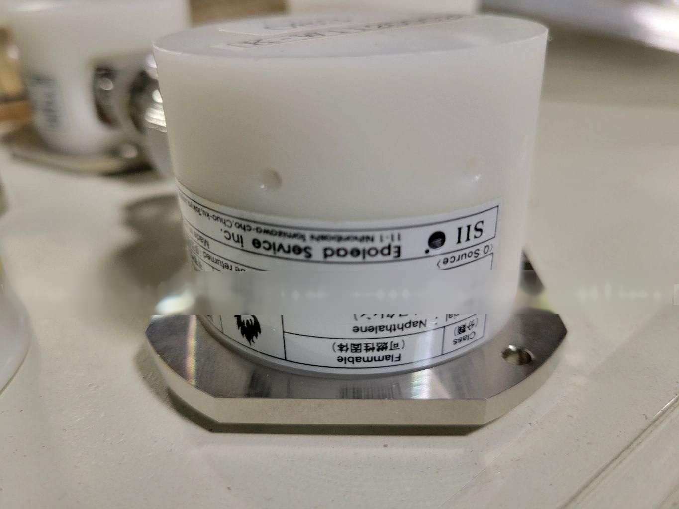
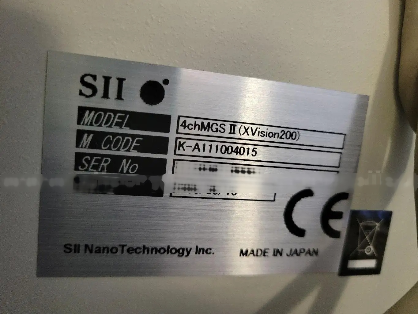
1ea 4chMGS II Gas control cabinet
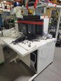
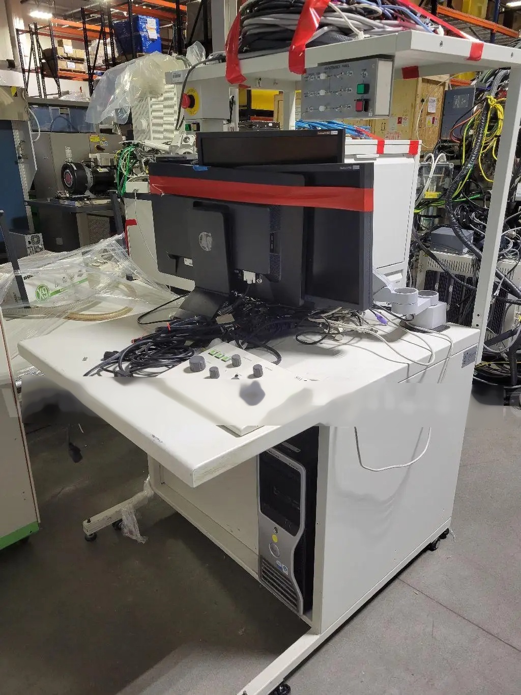
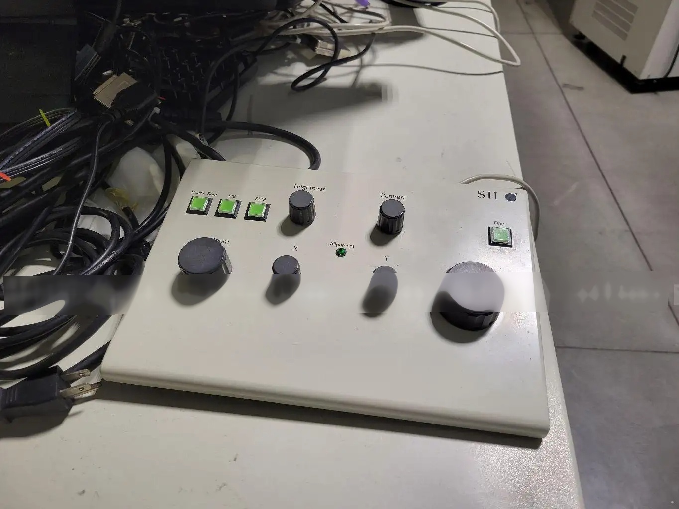
Control console
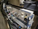
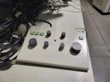
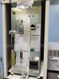
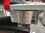
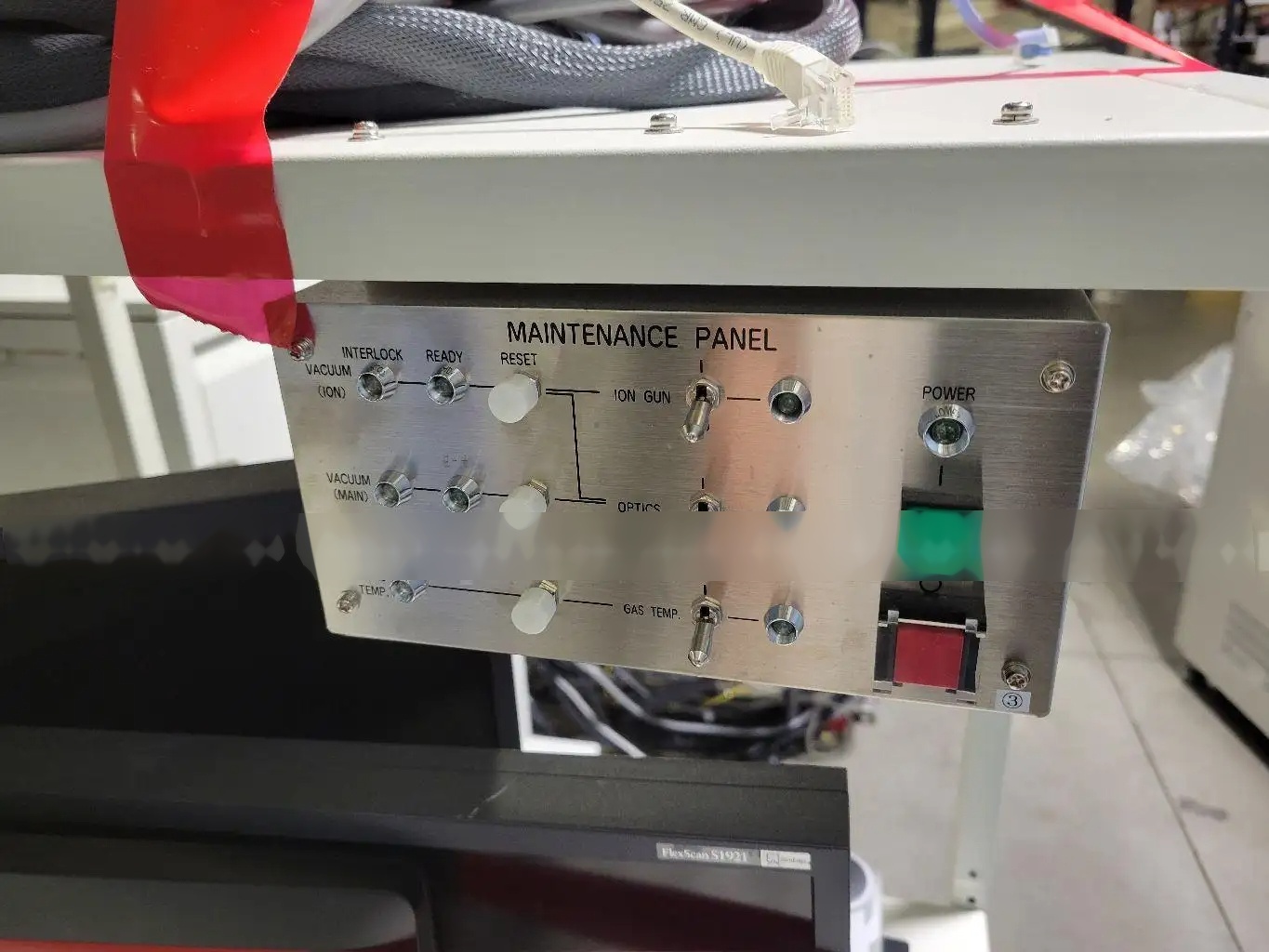
Maintenance panel
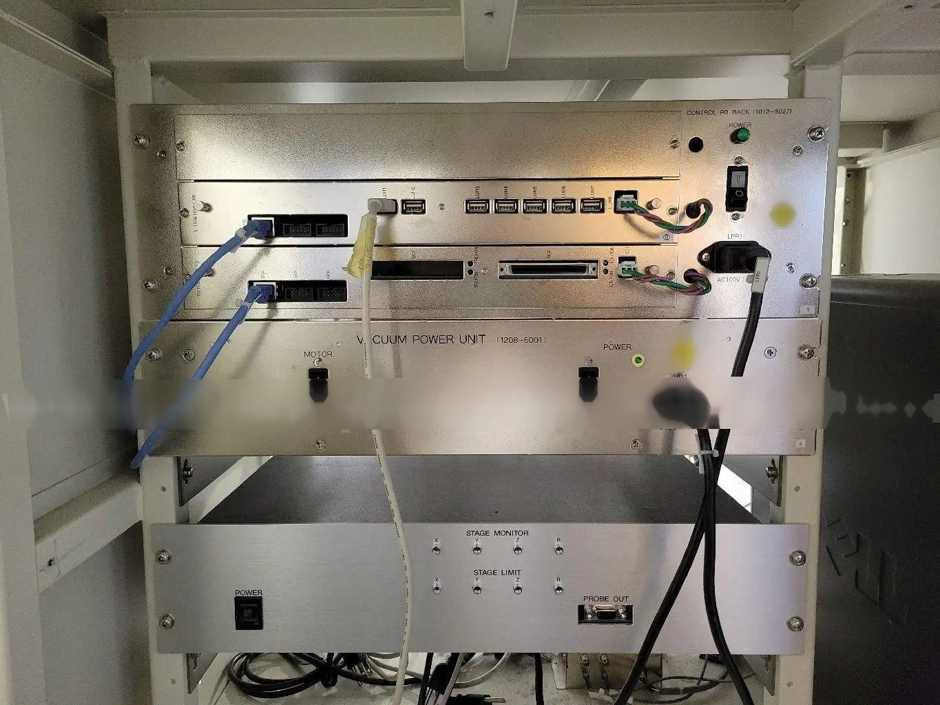
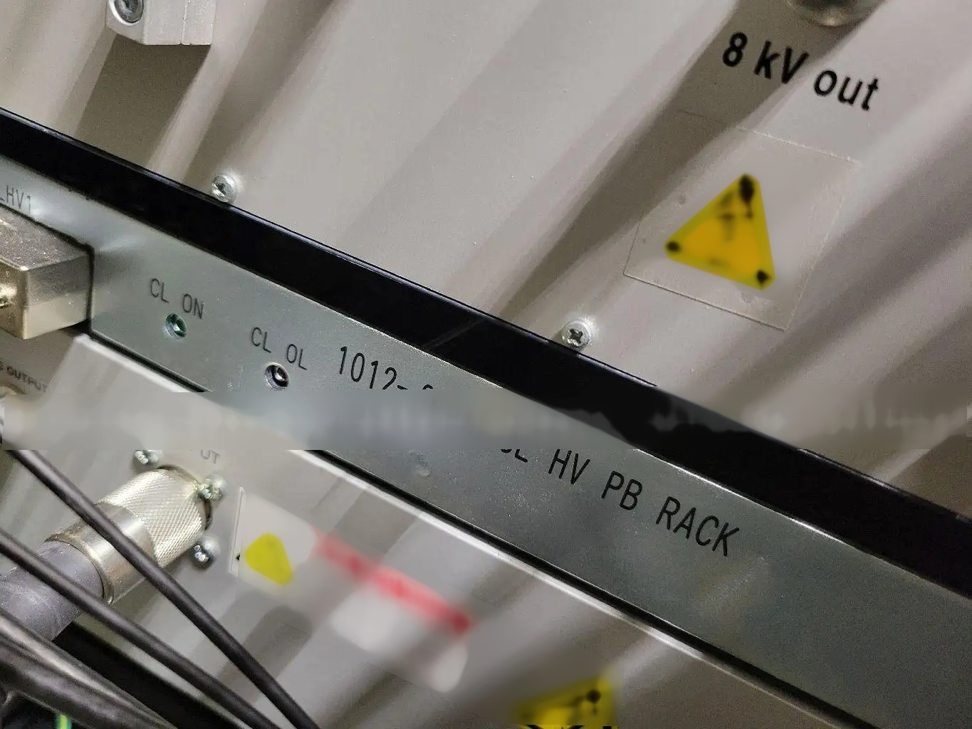
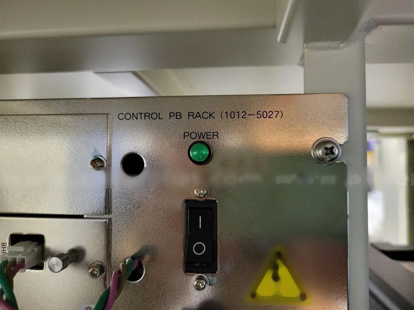
Control PB rack, P/N: 1012-5027
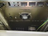
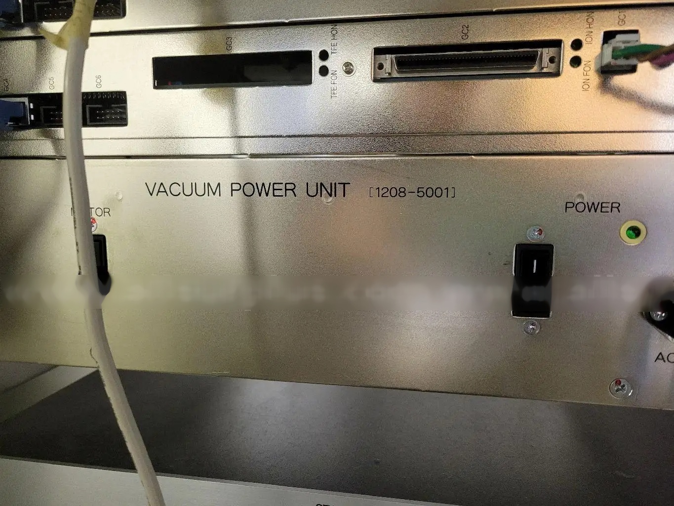
Vacuum power unit, P/N:1208-5001
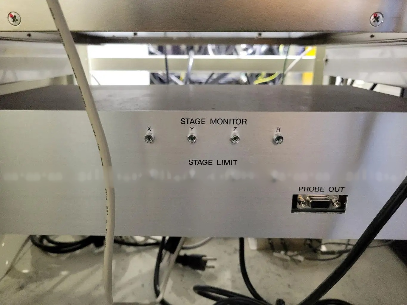
Stage monitor
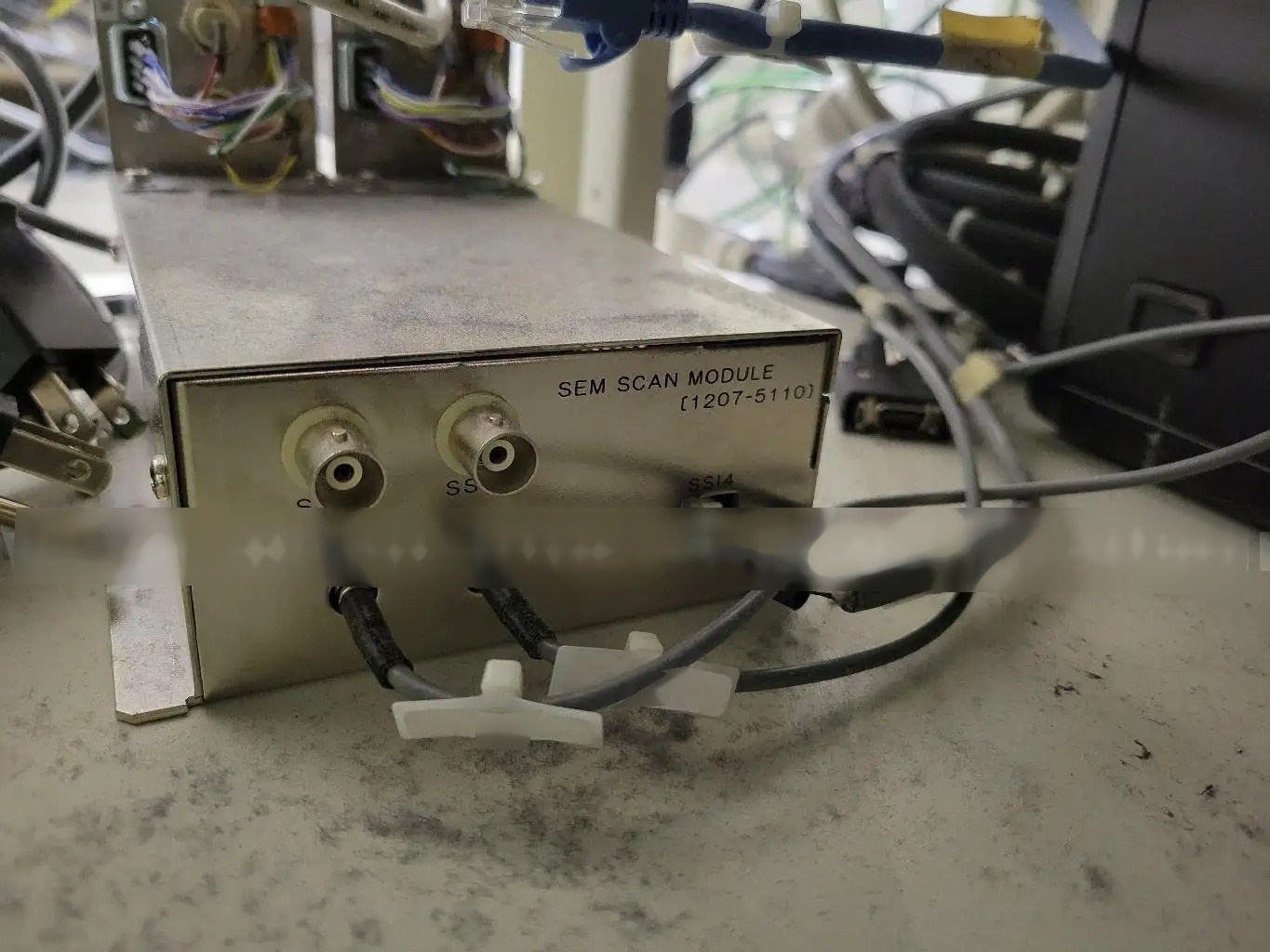
SEM Scan module, P/N: 1207-5110
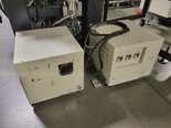
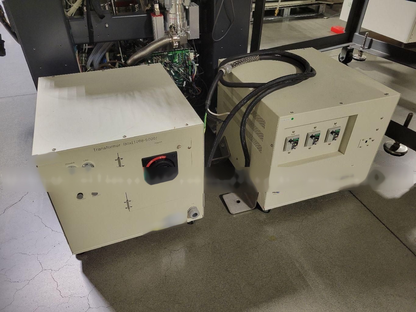
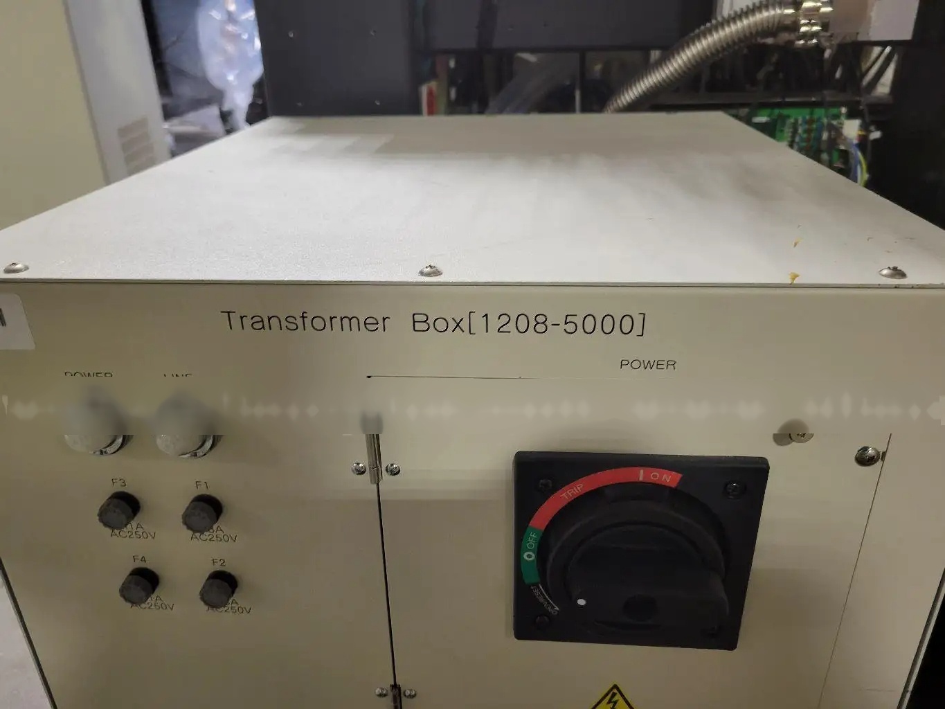
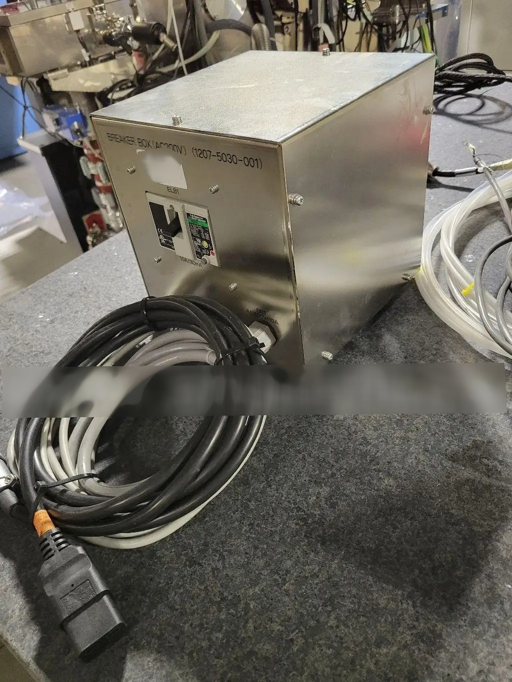
(2) Transformer boxes, P/N: 1208-5000
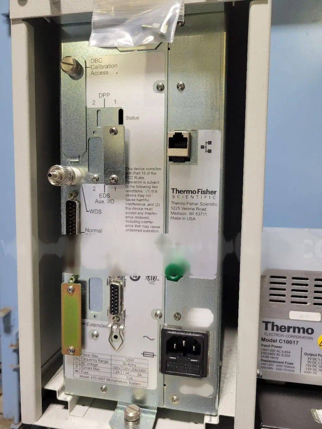
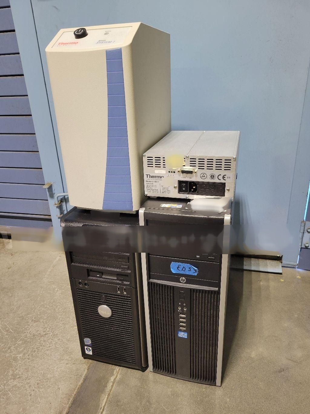
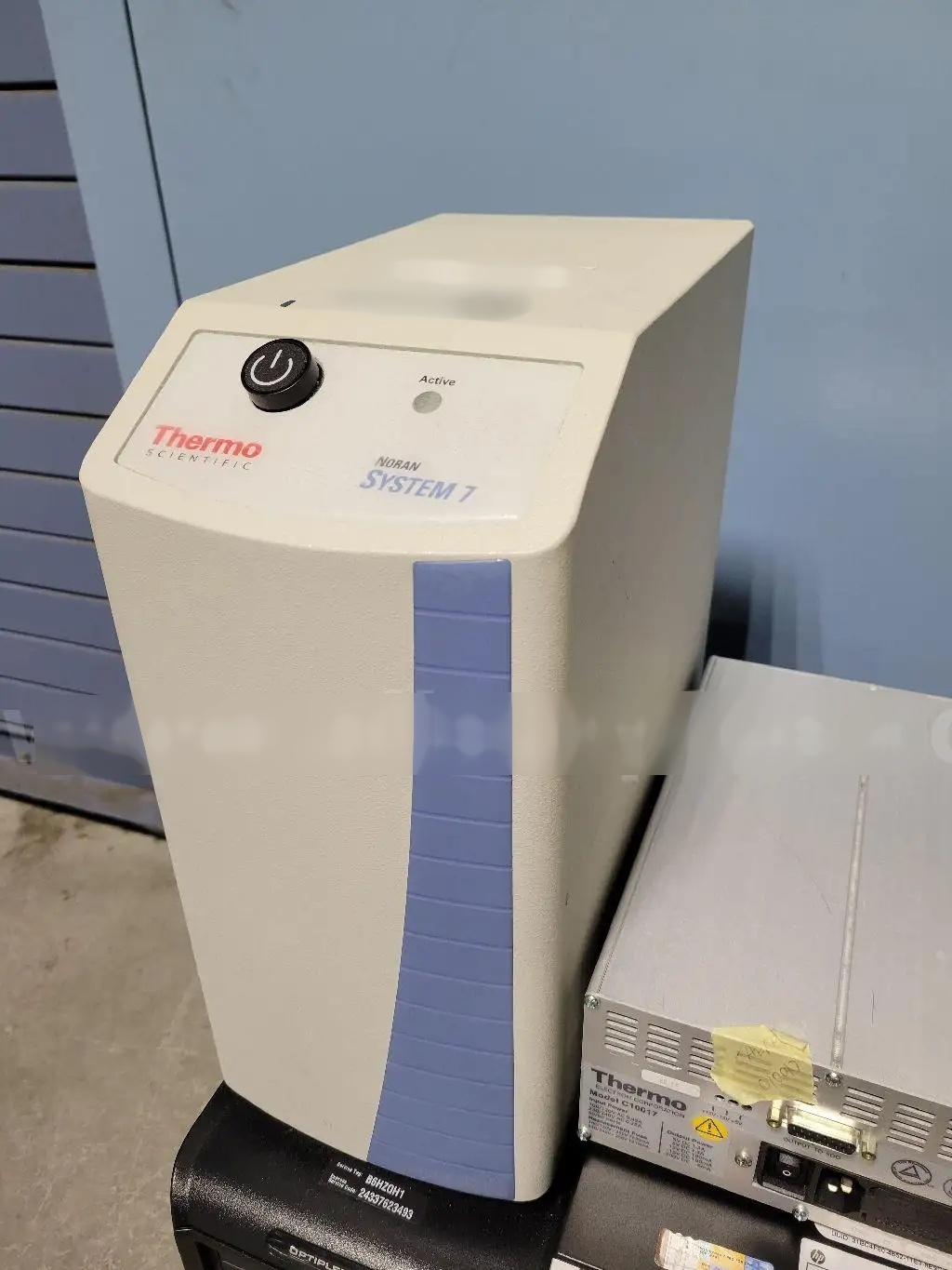
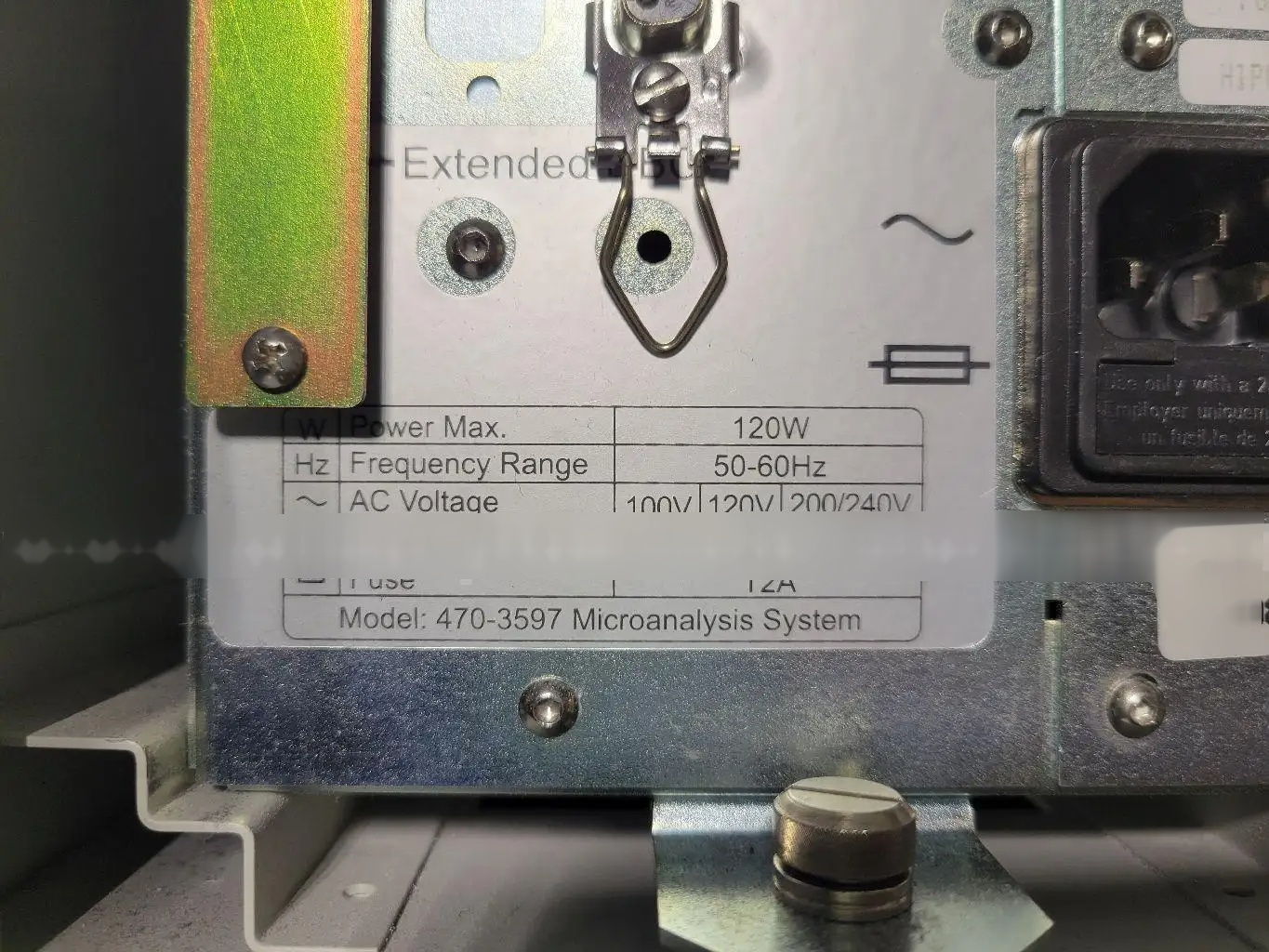
THERMO SCIENTIFIC NORAN SYSTEM 7 Microanalysis controller, P/N: 470-3597
Spare RAITH Beam blank controller
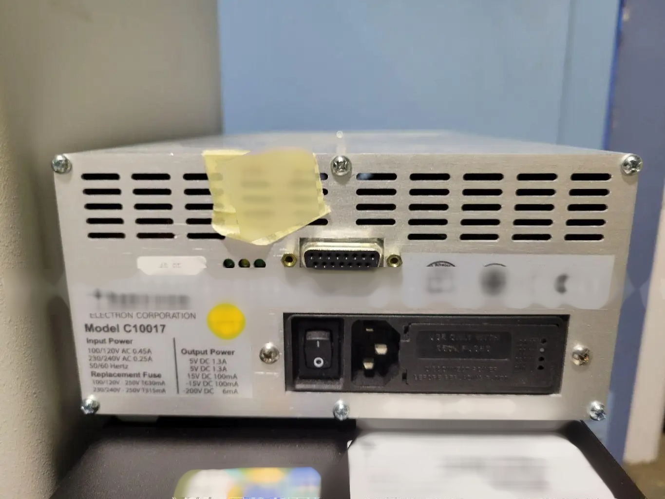
THERMO ELECTRON C10017 Silicon drift detector controller
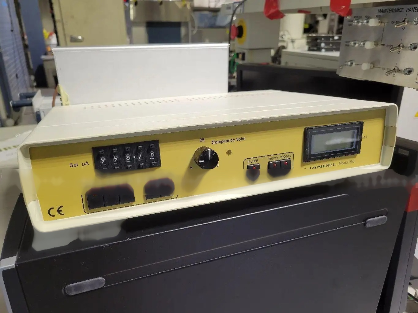
JANDEL RM2 4-point test controller
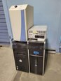
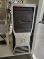
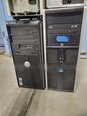
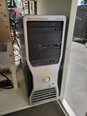
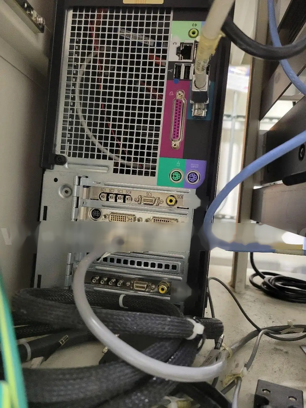
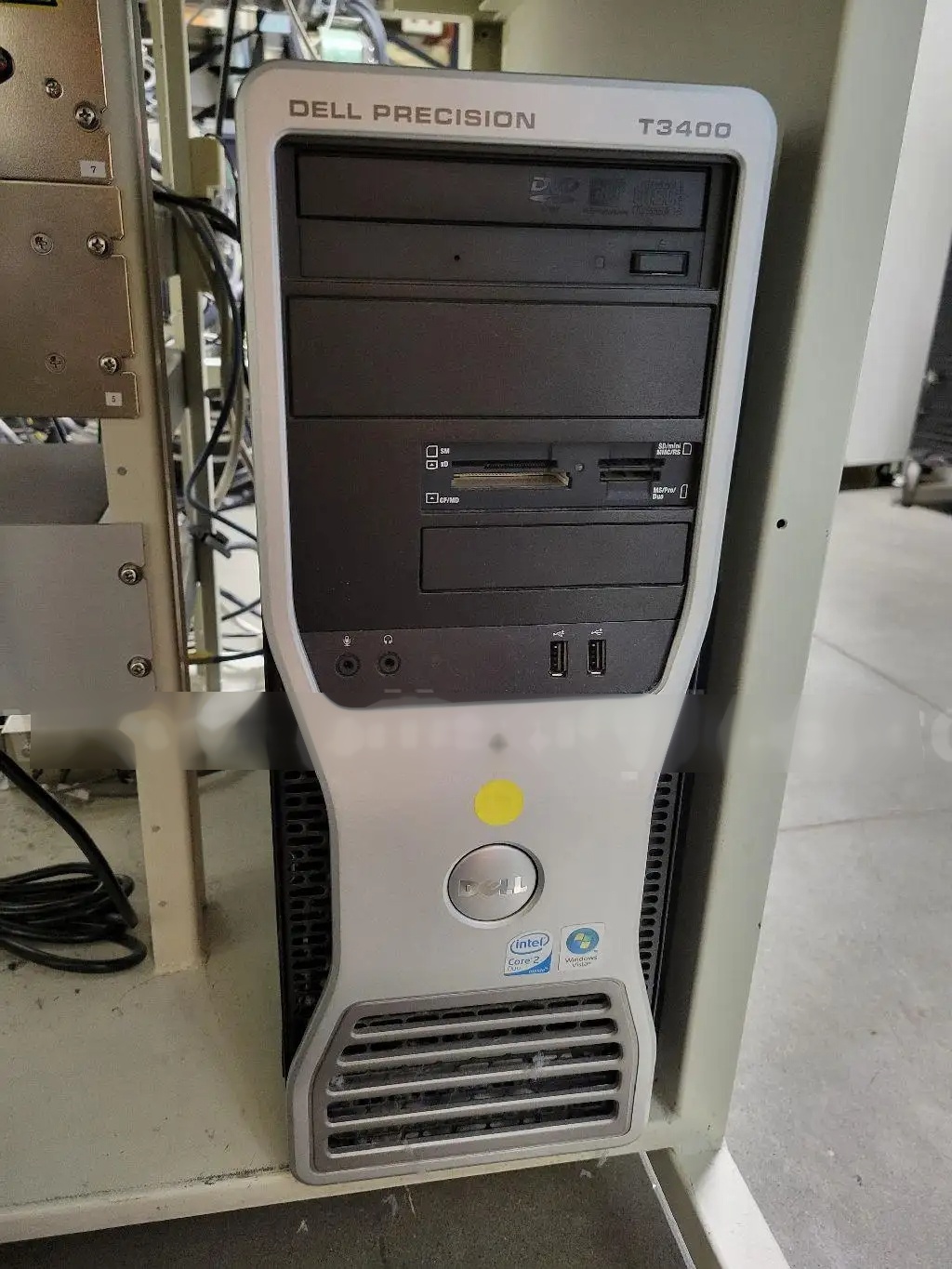
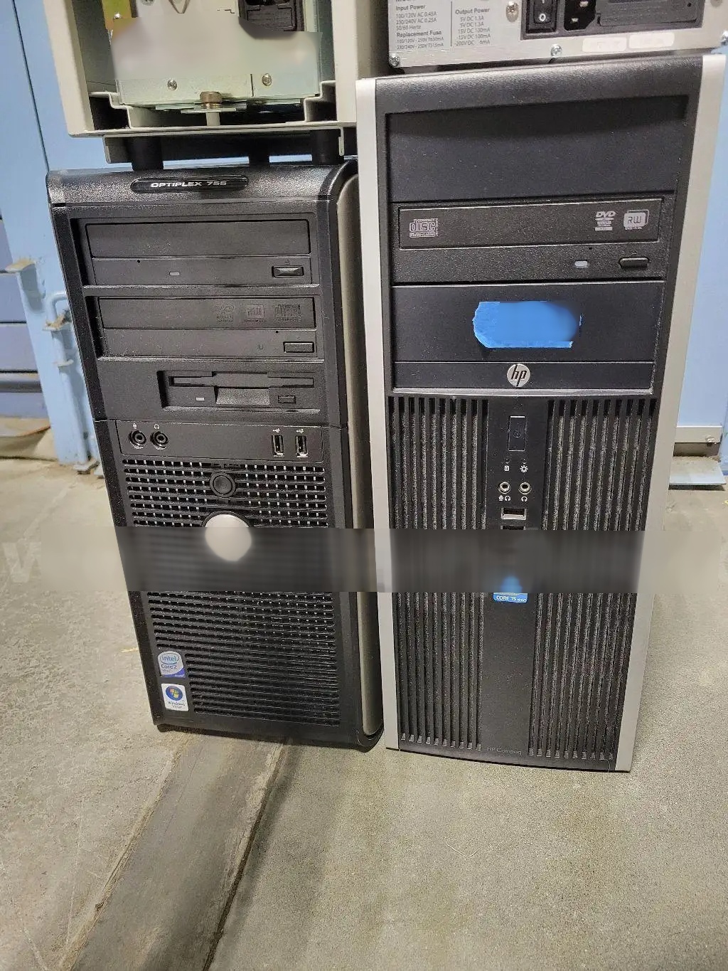
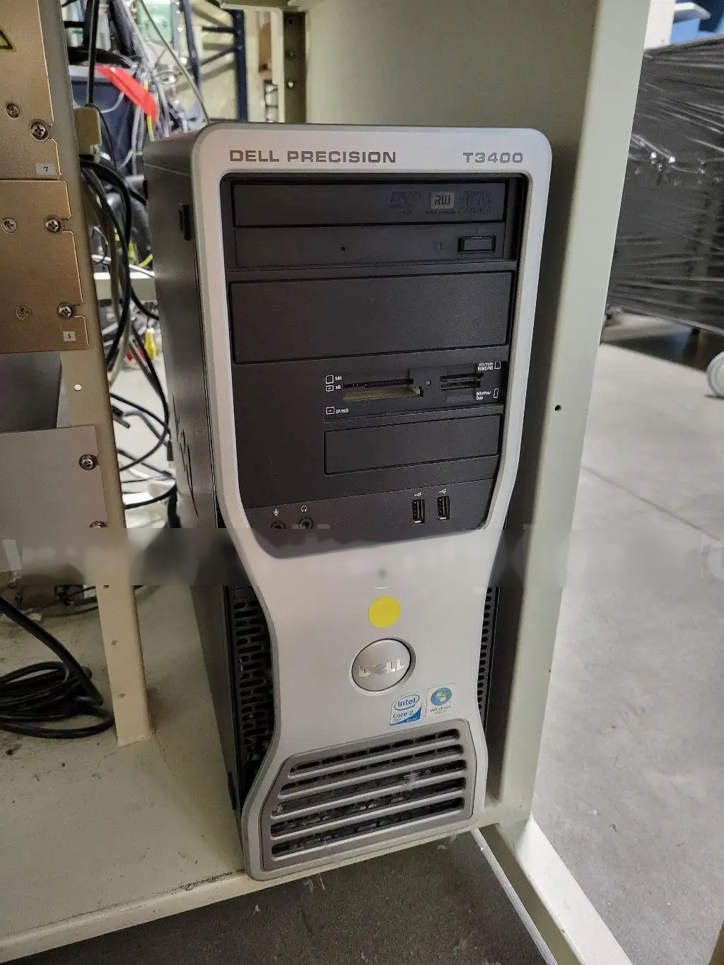
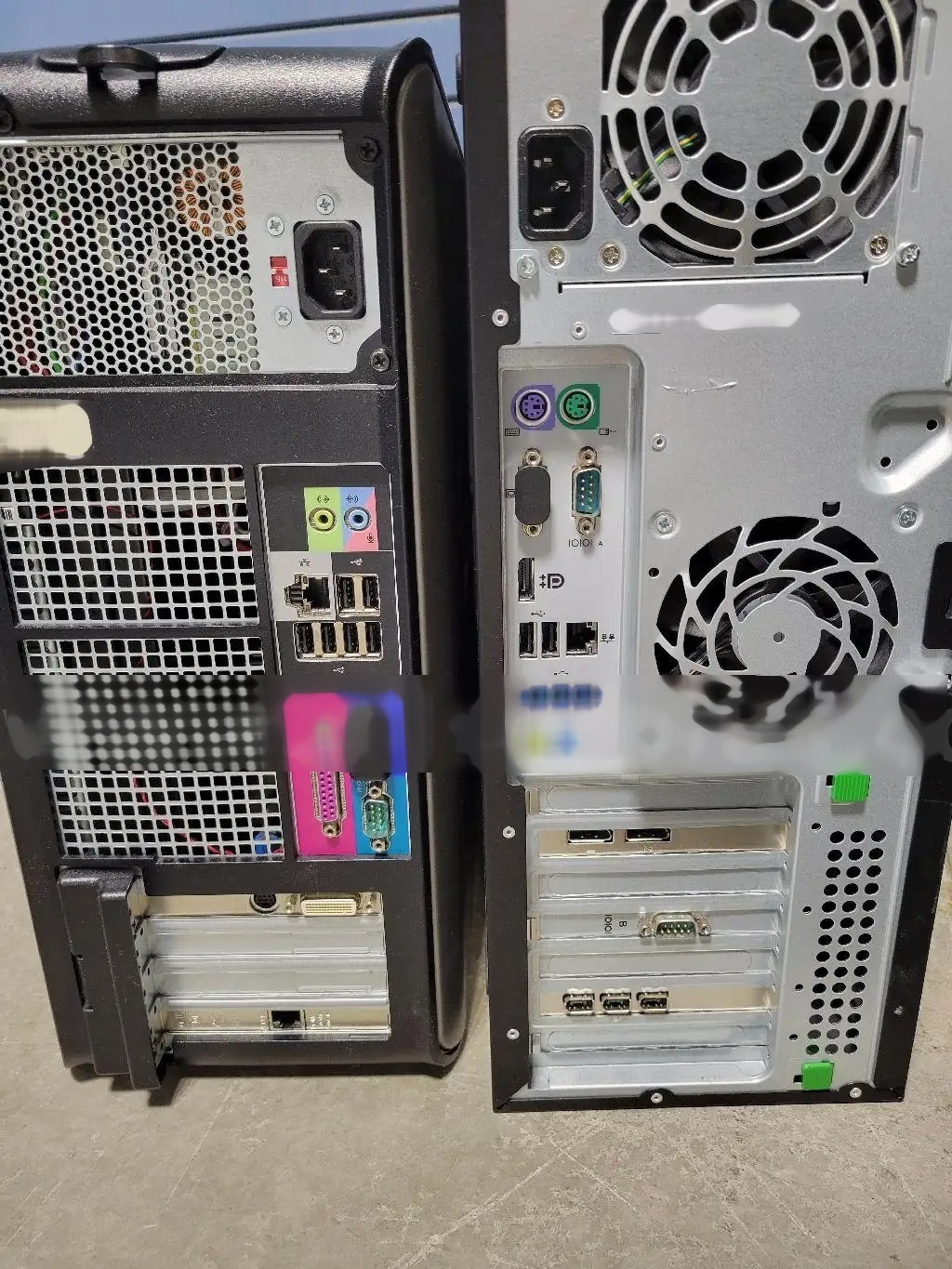
(3) PCs
No HDDs
2008 vintage.
SII NANO TECHNOLOGY X-Vision 200TB is a cutting-edge other wafer processing equipment designed to significantly enhance wafer processing capabilities in semiconductor manufacturing. This advanced system incorporates state-of-the-art nano-technology to achieve unparalleled levels of precision, efficiency, and scalability in the processing of semiconductor wafers. At the core of X-Vision 200TB unit is its innovative nano-technology, which enables ultra-high resolution imaging and precise manipulation of wafer surfaces at the nanometer scale. This level of precision is essential for achieving the strict dimensional requirements of modern semiconductor devices, such as transistors and memory cells. The machine utilizes advanced imaging technologies, including electron microscopy and atomic force microscopy, to accurately inspect and control wafer surfaces with nano-scale precision. Key features of SII NANO TECHNOLOGY X-Vision 200TB tool include a large processing capacity of 200 terabytes (TB), allowing for high-volume wafer processing to meet the demands of large-scale semiconductor production. The asset is equipped with multiple processing modules, each capable of handling a wide range of wafer sizes and materials, making it highly versatile and adaptable to various manufacturing processes. X-Vision 200TB model offers a comprehensive suite of processing capabilities, including precision etching, deposition, cleaning, and inspection, all integrated into a single platform for maximum efficiency and throughput. The equipment's advanced automation features enable seamless integration with existing manufacturing workflows, reducing processing time and improving overall yield rates. One of the key advantages of SII NANO TECHNOLOGY X-Vision 200TB system is its ability to perform multi-layer processing with exceptional precision and uniformity across the entire wafer surface. This level of control is critical for achieving optimal device performance and reliability in advanced semiconductor applications. Additionally, X-Vision 200TB unit incorporates advanced process monitoring and control algorithms to ensure consistent and repeatable results across multiple processing runs. Real-time feedback mechanisms continuously monitor processing parameters and make necessary adjustments to optimize process performance and yield. The machine is also designed with scalability in mind, allowing for easy integration of additional processing modules to meet evolving manufacturing requirements. This flexibility enables semiconductor manufacturers to expand their processing capabilities without significant disruptions to existing production lines. In conclusion, SII NANO TECHNOLOGY X-Vision 200TB represents a significant advancement in other wafer processing technology, offering unparalleled precision, efficiency, and scalability for semiconductor manufacturing applications. With its innovative nano-technology, high processing capacity, and comprehensive processing capabilities, X-Vision 200TB tool is poised to revolutionize wafer processing in the semiconductor industry and drive the development of next-generation semiconductor devices.
There are no reviews yet