Used SONY SI-C500 #293816184 for sale
URL successfully copied!
Tap to zoom
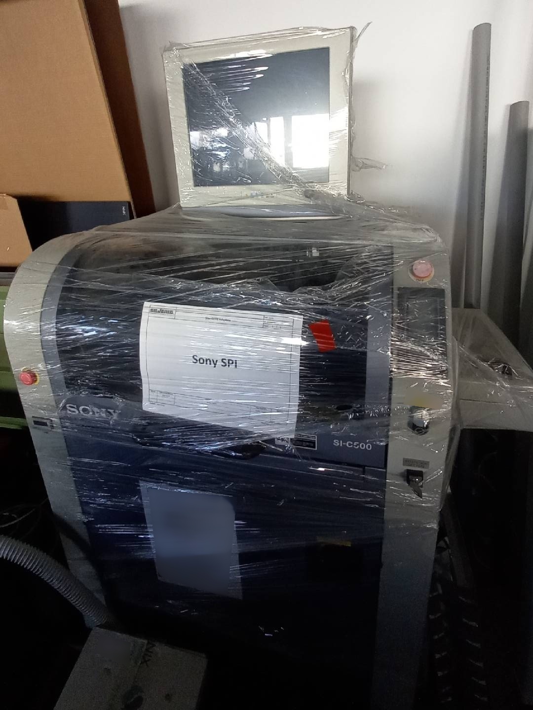

SONY SI-C500 is a cutting-edge wafer processing equipment designed for precision and efficiency in semiconductor manufacturing. As a leader in technology and innovation, SONY has developed this advanced system to meet the demanding requirements of the semiconductor industry. SI-C500 is part of the "other wafer processing" category, which involves various techniques and processes used in semiconductor fabrication beyond traditional lithography and etching. One of the key features of SONY SI-C500 is its high level of automation and advanced robotics capabilities. The unit is equipped with state-of-the-art robotic arms that can handle wafers with extreme precision and speed. This automation not only improves throughput and efficiency but also ensures consistent and reliable processing results. SI-C500 is designed to support a wide range of wafer sizes, from small substrates to larger wafers commonly used in advanced semiconductor manufacturing. This flexibility allows manufacturers to process different types of wafers without the need for extensive tooling changes, saving time and costs in production. In terms of processing capabilities, SONY SI-C500 offers a variety of functions to meet the diverse needs of semiconductor manufacturers. The machine is equipped with advanced cleaning modules that ensure the wafers are free from contaminants and particles before subsequent processing steps. This level of cleanliness is essential for achieving high yields and quality in semiconductor fabrication. Furthermore, SI-C500 includes precision cutting and dicing capabilities for wafer singulation and packaging. The tool can perform intricate cutting patterns with micron-level accuracy, ensuring that each die is separated cleanly and accurately from the wafer. This capability is crucial for the production of integrated circuits and other semiconductor devices that require precise die placement and alignment. In addition to cutting and dicing, SONY SI-C500 also features advanced inspection and metrology functions to ensure the quality and integrity of the processed wafers. The asset is equipped with high-resolution imaging sensors and measurement tools that can detect defects and deviations in wafer processing, allowing manufacturers to identify and address issues promptly. SI-C500 is designed with modularity and scalability in mind, allowing manufacturers to customize the model to their specific requirements. Whether it's adding additional processing modules, integrating new inspection tools, or upgrading robotic capabilities, the equipment can be easily adapted to accommodate changing production needs. From a software perspective, SONY SI-C500 is equipped with advanced control systems that enable seamless integration with existing manufacturing environments. The system can be easily programmed and controlled through user-friendly interfaces, allowing operators to monitor and adjust processing parameters in real-time. Overall, SI-C500 represents a cutting-edge solution for wafer processing in the semiconductor industry. With its advanced automation, precision capabilities, and versatility, the unit is well-suited for a wide range of applications, from cutting-edge integrated circuits to emerging semiconductor technologies. SONY continues to push the boundaries of semiconductor manufacturing with innovative solutions like SONY SI-C500, setting new standards for performance and quality in the industry.
There are no reviews yet