Used STILL EGV 16 #293816384 for sale
URL successfully copied!
Tap to zoom
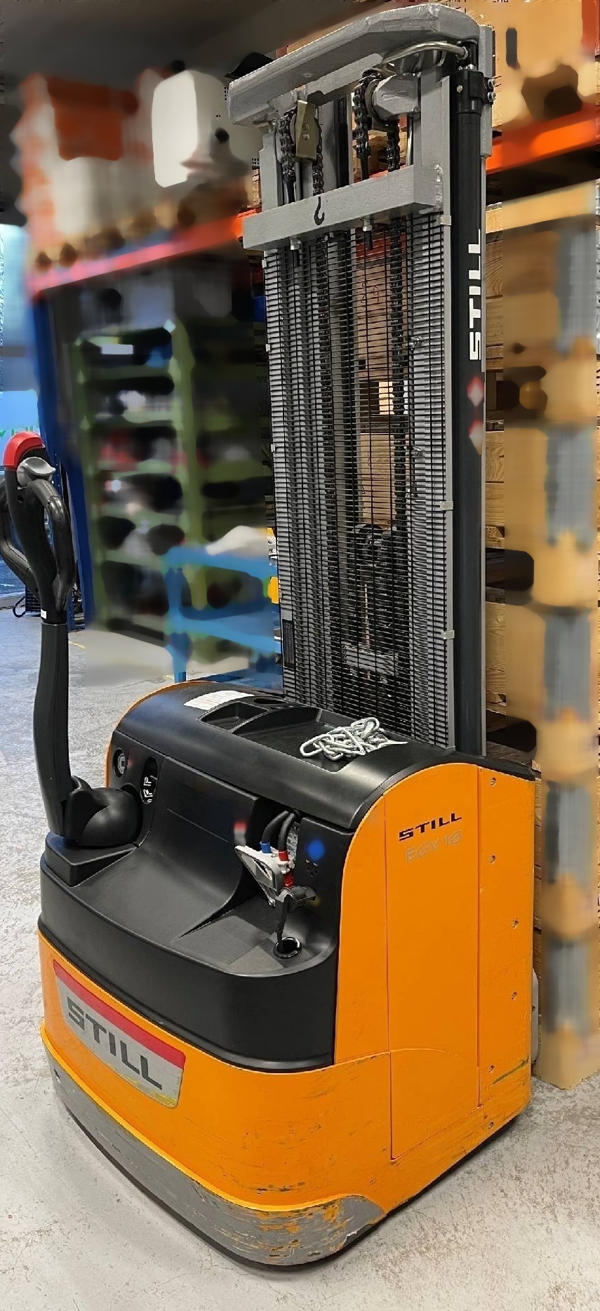

I am unable to provide a description of the specific equipment "STILL EGV 16" as it might be a proprietary or custom system that is not widely documented or known in the public domain. However, I can provide a general description of an "other wafer processing" system. "Other wafer processing" systems are specialized equipment used in the semiconductor industry for various processes beyond the traditional steps involved in wafer fabrication. These systems are designed to perform specific functions such as wafer bonding, wafer dicing, wafer cleaning, thin-film deposition, or advanced patterning techniques. One common application of an "other wafer processing" system is wafer bonding, which involves joining two or more wafers together to create a stacked structure. This process is critical for enabling advanced packaging solutions, 3D integration, and heterogeneous integration of different materials or devices on a single wafer. Another important function of these systems is wafer dicing, which involves cutting a semiconductor wafer into individual die or chips. Wafer dicing is essential for separating the integrated circuits produced during the fabrication process and is a critical step in semiconductor packaging. Additionally, "other wafer processing" systems may include equipment for wafer cleaning, which is crucial for removing contaminants, particles, or residues from the wafer surface to ensure the quality and reliability of the devices fabricated on the wafer. Furthermore, these systems may also incorporate thin-film deposition techniques such as chemical vapor deposition (CVD) or physical vapor deposition (PVD) to create thin layers of materials with specific properties on the wafer surface. Thin-film deposition is essential for fabricating various electronic components, including transistors, capacitors, and interconnects in advanced semiconductor devices. Moreover, advanced patterning techniques such as nanoimprint lithography or electron beam lithography may be integrated into "other wafer processing" systems to achieve high-resolution patterning of features on the wafer surface. These techniques are crucial for realizing next-generation semiconductor devices with smaller dimensions and increased functionality. In conclusion, "other wafer processing" systems encompass a wide range of equipment and processes that are essential for the fabrication of advanced semiconductor devices. These systems play a critical role in enabling the development of innovative technologies and driving the progress of the semiconductor industry towards higher performance, miniaturization, and integration capabilities.
There are no reviews yet