Used TORAY Titler #293826765 for sale
URL successfully copied!
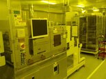
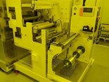
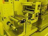
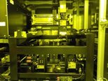
Tap to zoom
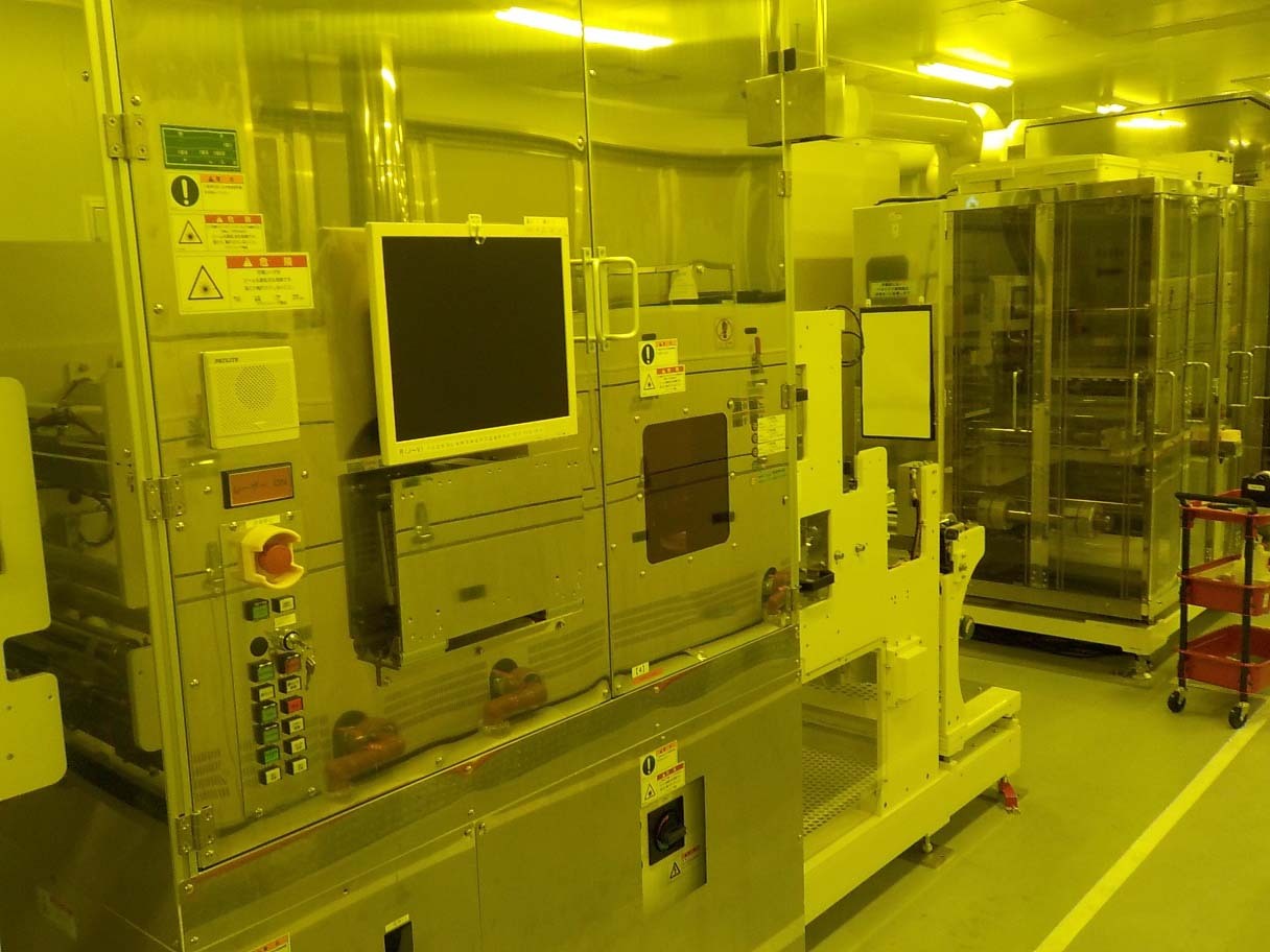

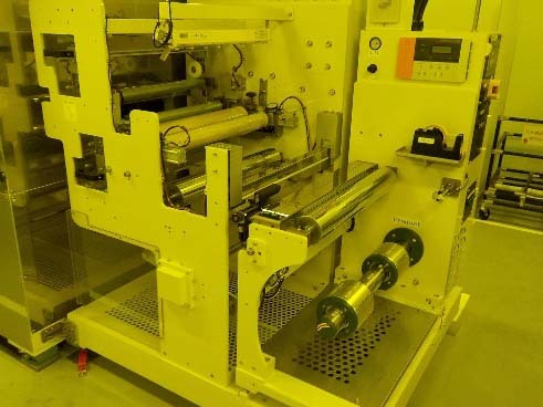
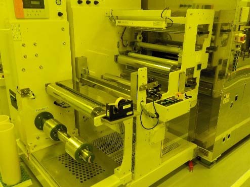
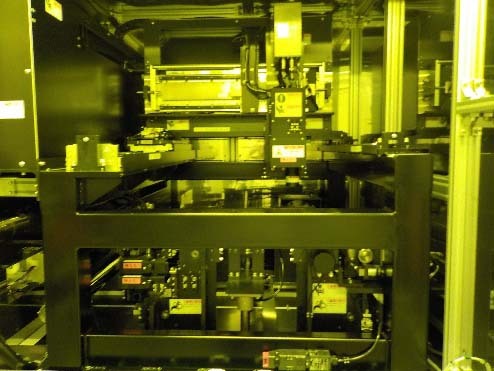
ID: 293826765
Laser
Exposure head
Patterning method: Optical mask method
Exposure range: Entire workpiece
Printing direction: 0, 90, 180, 270°
Character / string tilt: Within ±3°
Character line width: 30 µm
Exposure position accuracy: ±150 µm
Exposure illuminance: Over 1200 mW/cm² (405nm)
Illuminance meter: USHIO (UIT201, UVD-405PD)
Illuminance uniformity: Guaranteed value ±20%
Exposure wavelength: h-line (405 nm)
Light source: Laser diode
Focus depth: ±0.5 mm.
As an SEO specialist, I need to clarify that the term "TORAY Titler" does not have any specific technical definition or known reference in the field of wafer processing systems. It seems to be a specific product or tool from a company named TORAY, but without detailed information or specifications available, it is challenging to provide a technical description. However, I can offer a general overview of wafer processing systems and explain key components and processes typically involved in such systems to give you an idea of what a system like Titler might entail. Wafer processing systems are essential equipment used in the semiconductor industry for the fabrication of integrated circuits on silicon wafers. These systems play a crucial role in the production of semiconductor devices by performing various processes such as deposition, etching, lithography, and inspection on the wafer surface. One of the primary components of a wafer processing system is the wafer handling mechanism, which is responsible for loading and unloading wafers onto the processing chamber. This mechanism ensures that the wafers are properly aligned and secured during the processing steps to maintain accuracy and consistency. Deposition processes involve the deposition of thin films of materials such as metals, dielectrics, or semiconductors onto the wafer surface. This can be done through techniques like chemical vapor deposition (CVD), physical vapor deposition (PVD), or atomic layer deposition (ALD). These processes are critical for creating the various layers and structures needed for semiconductor devices. Etching processes are used to selectively remove material from the wafer surface to create patterns and features. Common etching techniques include wet etching and dry etching, which use chemical or plasma-based processes to achieve high precision and control over the etched features. Lithography is a key process in semiconductor manufacturing that involves transferring patterns from a mask onto the wafer surface. This process uses photolithography techniques, where UV light is used to expose a light-sensitive photoresist layer on the wafer, allowing for precise patterning of features at the nanoscale level. Inspection and metrology are crucial steps in wafer processing systems to ensure the quality and integrity of the fabricated semiconductor devices. Advanced imaging techniques, such as scanning electron microscopy (SEM) and optical inspection, are used to examine the wafer surface for defects, impurities, or deviations from design specifications. Overall, wafer processing systems are highly complex and sophisticated equipment that require precision engineering, advanced automation, and stringent process control to achieve high yields and quality in semiconductor manufacturing. As a specialist familiar with SEO best practices, I recommend that you provide more specific details or technical specifications of TORAY Titler system to create relevant and optimized content for your target audience.
There are no reviews yet