Used ACCRETECH / TSK FP 3000 #293760840 for sale
URL successfully copied!
Tap to zoom

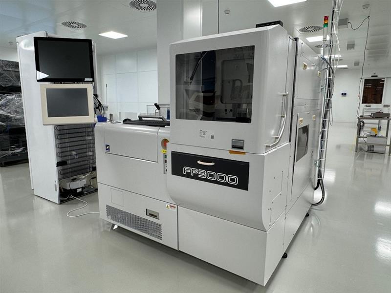
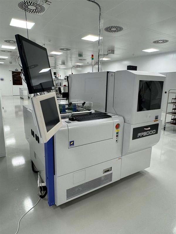
ID: 293760840
Wafer Size: 8"-12"
Prober, 8"-12"
Automatic probe
Automatic needle height alignment
Frame loader, 12"
Standard loader, 8"
Ceramic with touch sensor
Needle cleaning stage: 160 x 160 mm
Multi-pass probing
Process: SECS / GEM
Probe card holder
XANDEX Inker
FMI (Ink dot inspection)
Loader cover
Joystick
Capacitance profile sensor
Probe Mark Inspection (PMI)
CE Marked
Interface:
GPIB
Ethernet
Head plate opening prepared cable
RS232.
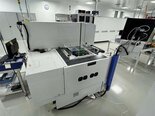
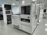
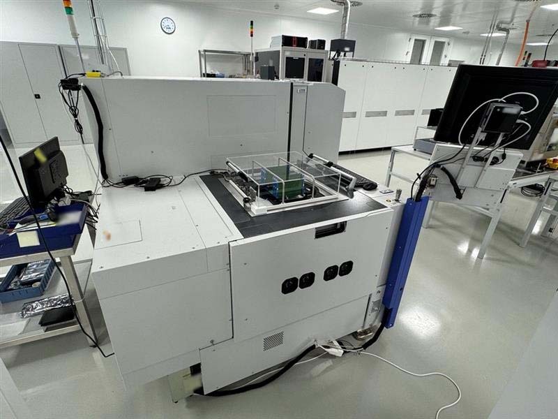
ACCRETECH / TSK FP 3000 Prober is a state-of-the-art device used to check the quality of a semiconductor chip. The device is composed of an TSK Probing Equipment Mainframe (PEM)-S with a Dual probing head, a multi-axis step motor platform for positioning the probe head in the test station, a vision equipment for monitoring and verifying the probe position and alignment for multiple marker points, a vision inspection area for inline In-Circuit Test (ICT), an opto-isolator test area, and an Automatic Tool Change (ATC) system. ACCRETECH Probing Equipment mainframe (PEM)-S is the primary unit of the prober and comprises a microcontroller, a high-speed controlling factor, a CNC unit, and a high speed positioning machine. The microcontroller is responsible for controlling the motion, speed, and position of the probe head, while the CNC tool provides faster and smoother operation even with higher probing frequencies. The high-speed controlling factor enables the asset to attain a high precision when probing multiple points. The high-speed positioning model ensures precise movement and positioning accuracy of the probe head. The Dual probing head is composed of two high-precision and high-resolution probing heads. This design provides a high degree of versatility allowing for a greater array of test scenarios to be conducted. The heads are also equipped with a pressure feedback equipment that can provide information on wear and electrode degradation; this helps to ensure accuracy and quality of test results. The multi-axis step motor platform enables the probe heads to be positioned accurately within the test station. The system utilizes a de-magnetization agent to reduce noise and ensure high positioning precision. This provides repeatability when probing larger chip areas where multiple positioning measurements need to be taken. The vision unit is used to monitor and verify the probe position and alignment for multiple marker points. This ensures that the probes are accurately placed on the desired test contacts and that probe tips are not damaged on the surface of the device under test. Additionally, the vision machine is able to detect shorts, breakage, abnormality and other defects. The vision inspection area allows for inline In-Circuit Test (ICT) which verifies the operation and quality of the semiconductor device. This tool utilizes a combination of barrel and vision probes and can determine the presence of faults in the experimental circuit. The opto-isolator test area allows for stricter testing of the device under test in order to prevent leakage and short circuit conditions. This asset is capable of measuring the isolation impedance of each isolated node on the device which greatly improves overall chip functionality and reliability. Finally, the Automatic tool change model provides a flexible platform for quick and easy to changeover of various types of tools. This allows the prober to optimize the process parameters according to the device under test thereby ensuring the highest possible testing accuracy and quality.
There are no reviews yet