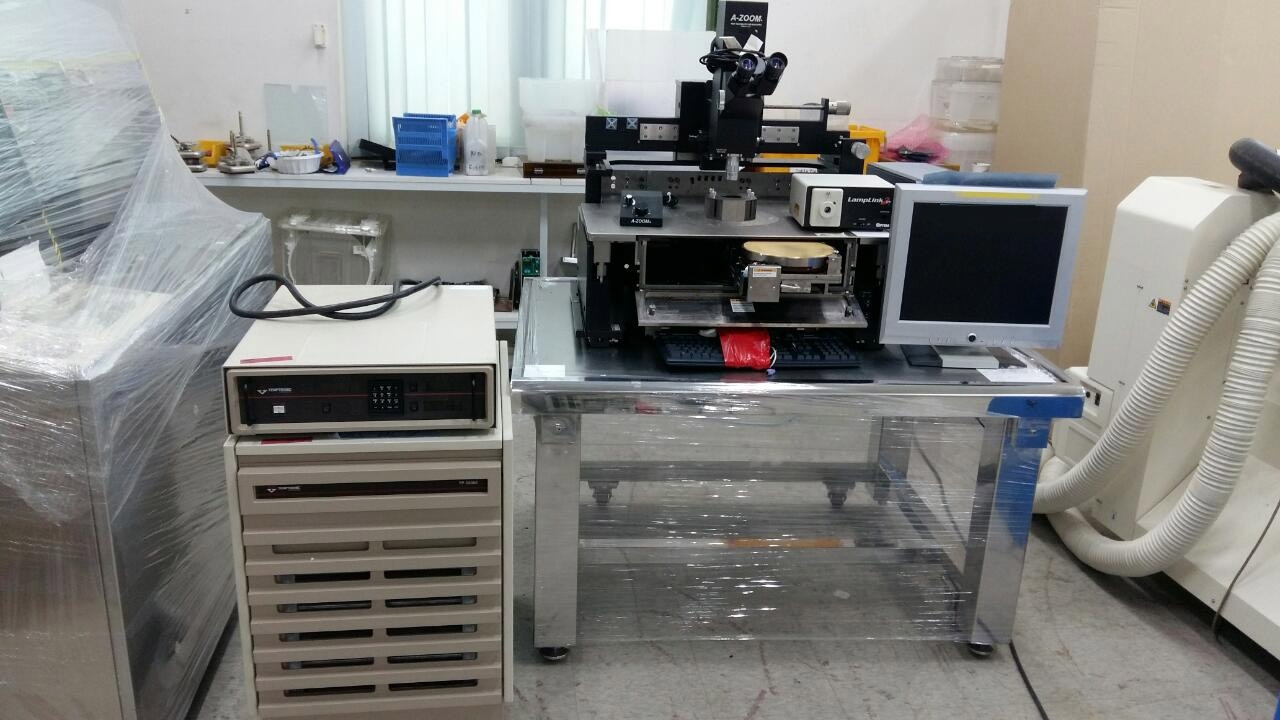
Used CASCADE MICROTECH / ALESSI Summit 11000 #9209218 for sale
It looks like this item has already been sold. Check similar products below or contact us and our experienced team will find it for you.
Tap to zoom


Sold
ID: 9209218
Wafer Size: 8"
Probers, 8"
Cold capability
With TEMPTRONIC chiller
Typical height to eye pieces: 55 cm
Platen:
Rigdity: <50-Micron (2 mil) for 4.5 kg lateral / Vertical force
Z-Litt range: 5.5 mm (0.22") Linear lift
Z-Lift repeatability: <2-Micron (0.08 mil)
Material: Nickel plated steel
Rotary stage:
Travel: ±7°
Resolution: 1° per Turn
Roll-out stage:
Travel: 25 cm
Chuck:
Size: 200 mm
Diameter: 150 mm Stations
Surface: Gold-plated / Nickel-plated aluminum
With provisions for grounding / Biasing
X-Y Stage:
Travel: 203 mm x 203 mm
Resolution: 0.2" Per turn
Bearings: Cross-roller
Micro chamber:
EMI Isolation
Light tight
Enclosure: Dry air & inert gas purge capable
Maximum positioners: (8) DCM (Seven with high-power microscope) / (4) RF
Chuck specifications:
Flatness: 0.39 mils (10 Microns) Across total surface
Isolation & chuck to shield: > 10Ω
Auxiliary chucks: Two with Individual vacuum controls
Breakdown bias voltage: > 1000 Volts
Vacuum distribution area: 13, 75/152 mm (Selectable)
Total system planartiy:
<20-Mlcron (0.8 mil) across 101 mm
Circle: 4"
<30-Micron (1.2 mil) across 203 mm
Circle: 8".
CASCADE MICROTECH / ALESSI Summit 11000 is a prober designed for parameterizing, analyzing, and measuring semiconductor devices, substrates, and circuits on wafers. The prober is equipped with a precision motion control equipment that enables it to accurately move the wafer or sample from one measurement point to the next. ALESSI Summit 11000 combines an XYZ stages with a triple-axis inclinometer for precise alignment and motion control. It also features a vertical load-leveling feature to improve alignment of the sample with the needles. The prober features a high-resolution, high-dynamic imaging system that consists of fast response time cameras, image capture, illumination control, and auto-focus algorithms. This imaging unit is designed for improved wafer mapping, automated image alignment, and double exposure. CASCADE MICROTECH Summit 11000 also includes an optimized automated probing process which is capable of measuring contact resistors, test points, and external connections. The prober is powered by a Windows-based graphical user interface and can integrate with other tools like Waferhound, Spike, and Configure & Connect. With Waferhound, users can quickly acquire meaningful data for debugging and analysis. Spike allows for automated prober status logging. Configure & Connect enables remote, secure access to the prober over the network. Summit 11000 may also be configured for different types of measurements, including sheet resistance, on-resistance, device parameters, substrate parameters, and device characterization. The optional Integrated Test Network allows for multiple device testing, visibility into die and probe information, and full execution of advanced device characterization methods. The prober is designed to integrate with other tools, allowing for advanced integration with Wafer Level Reliability (WLR) testing tools. It can also box measure for enhanced accuracy. CASCADE MICROTECH / ALESSI Summit 11000 is intended for high reliability and high productivity in the semiconductor test industry. It features reliability engineering features such as a built-in temperature monitoring machine, a repeatable alignment mechanism, and high-resolution cleaning needles. Additionally, the prober helps engineers reduce cycle time and production cost with its automated probing algorithms.
There are no reviews yet