Used ELECTROGLAS / EG 2001X #293797075 for sale
URL successfully copied!
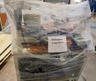
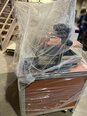
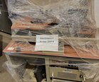
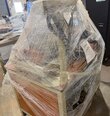
Tap to zoom
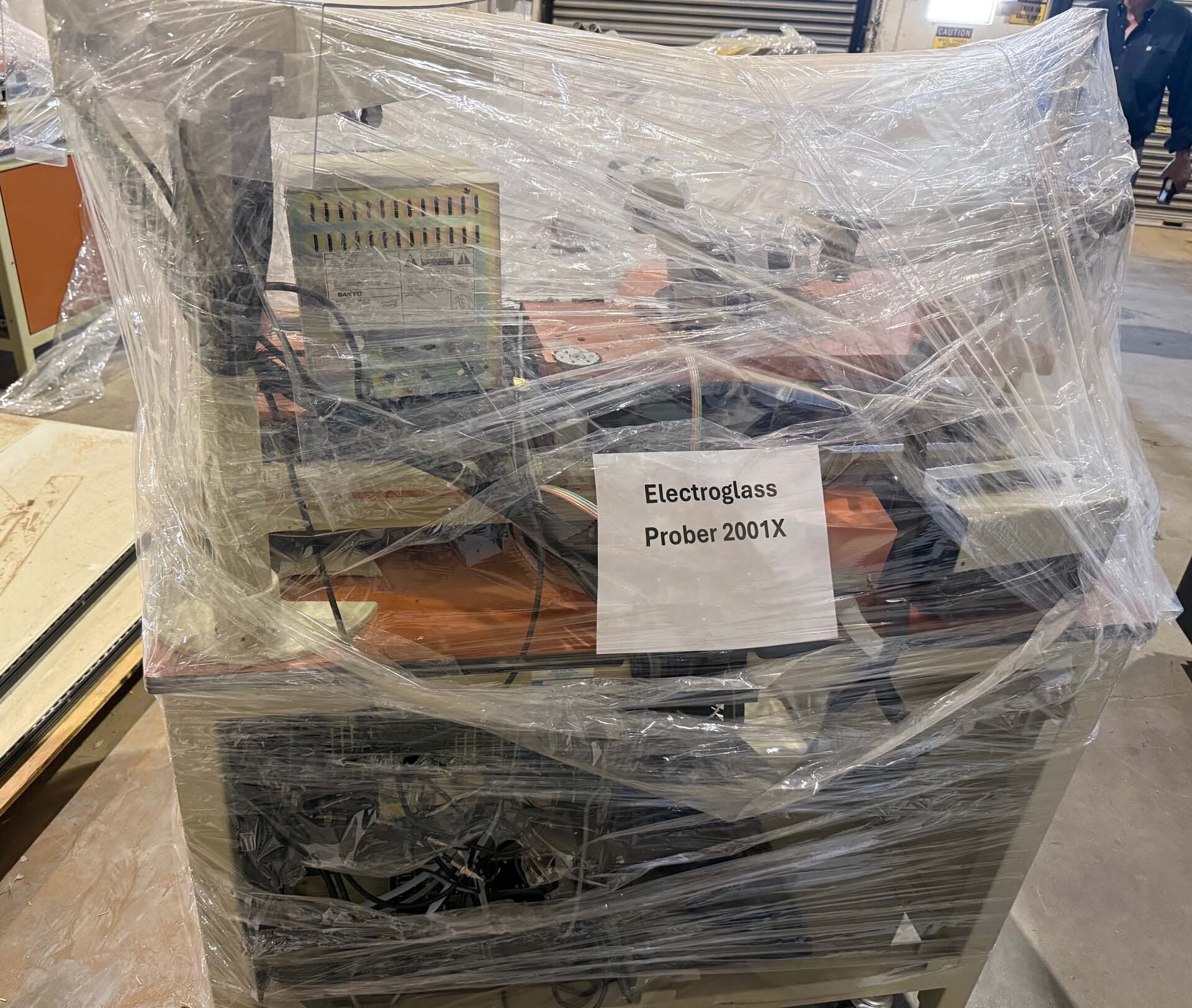

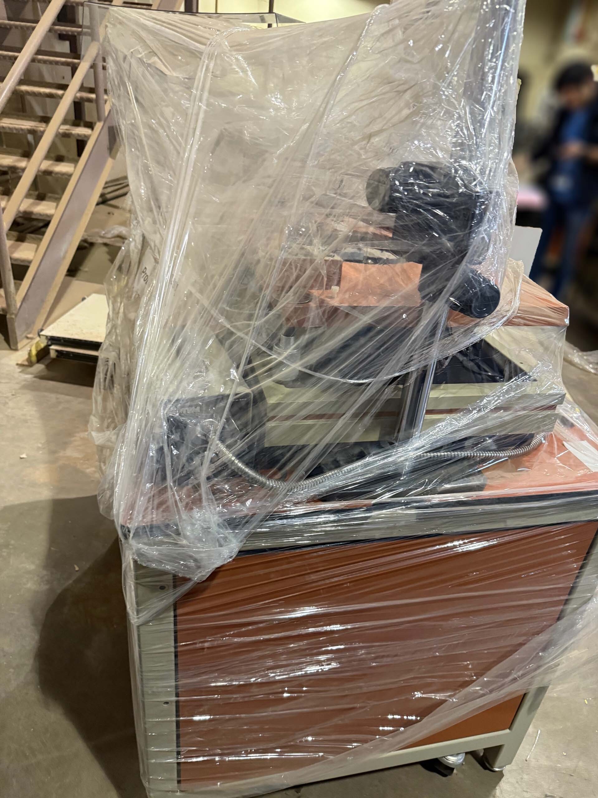
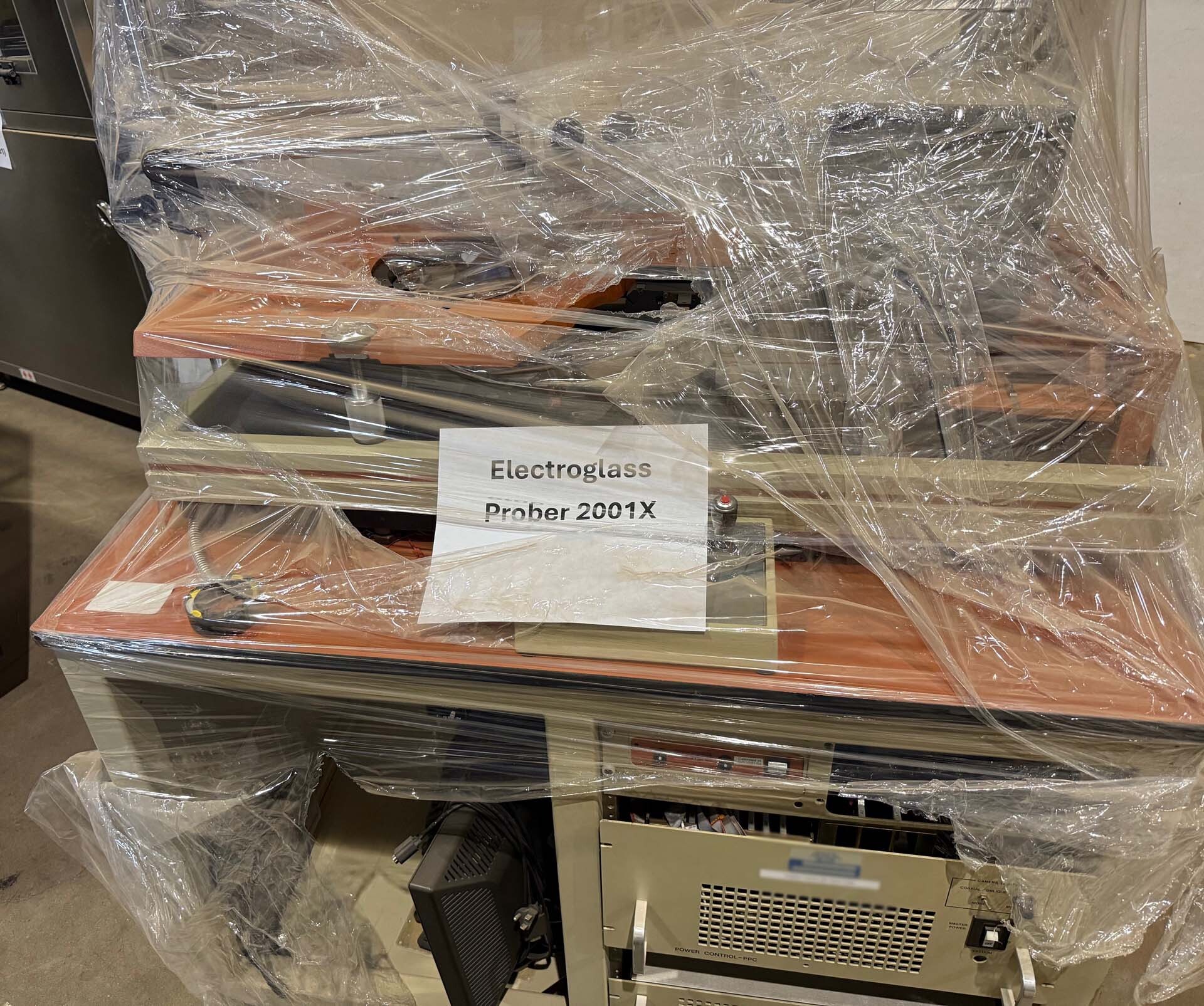
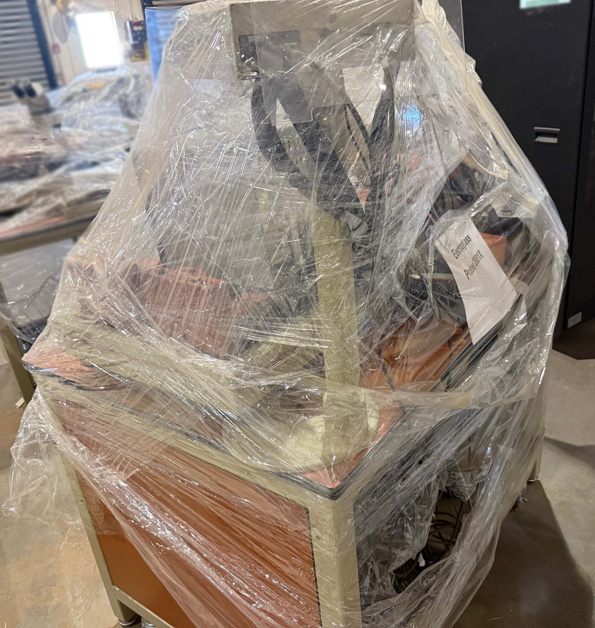
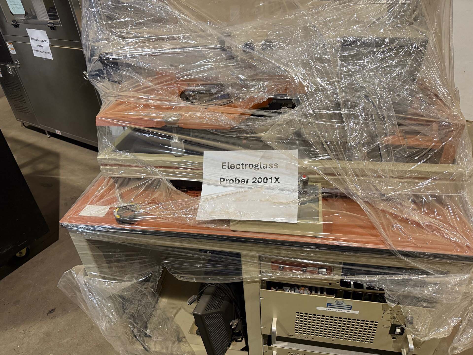
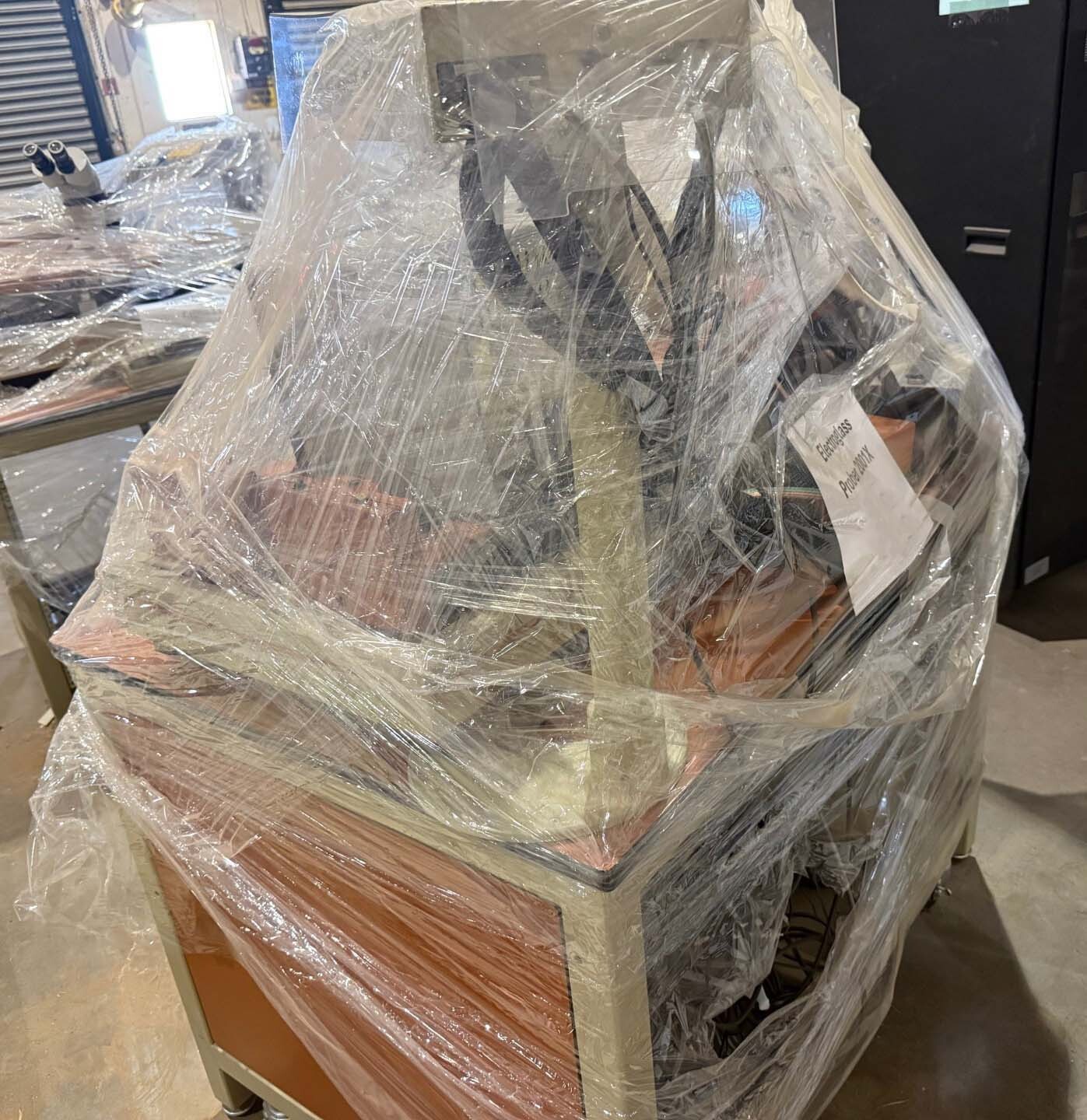
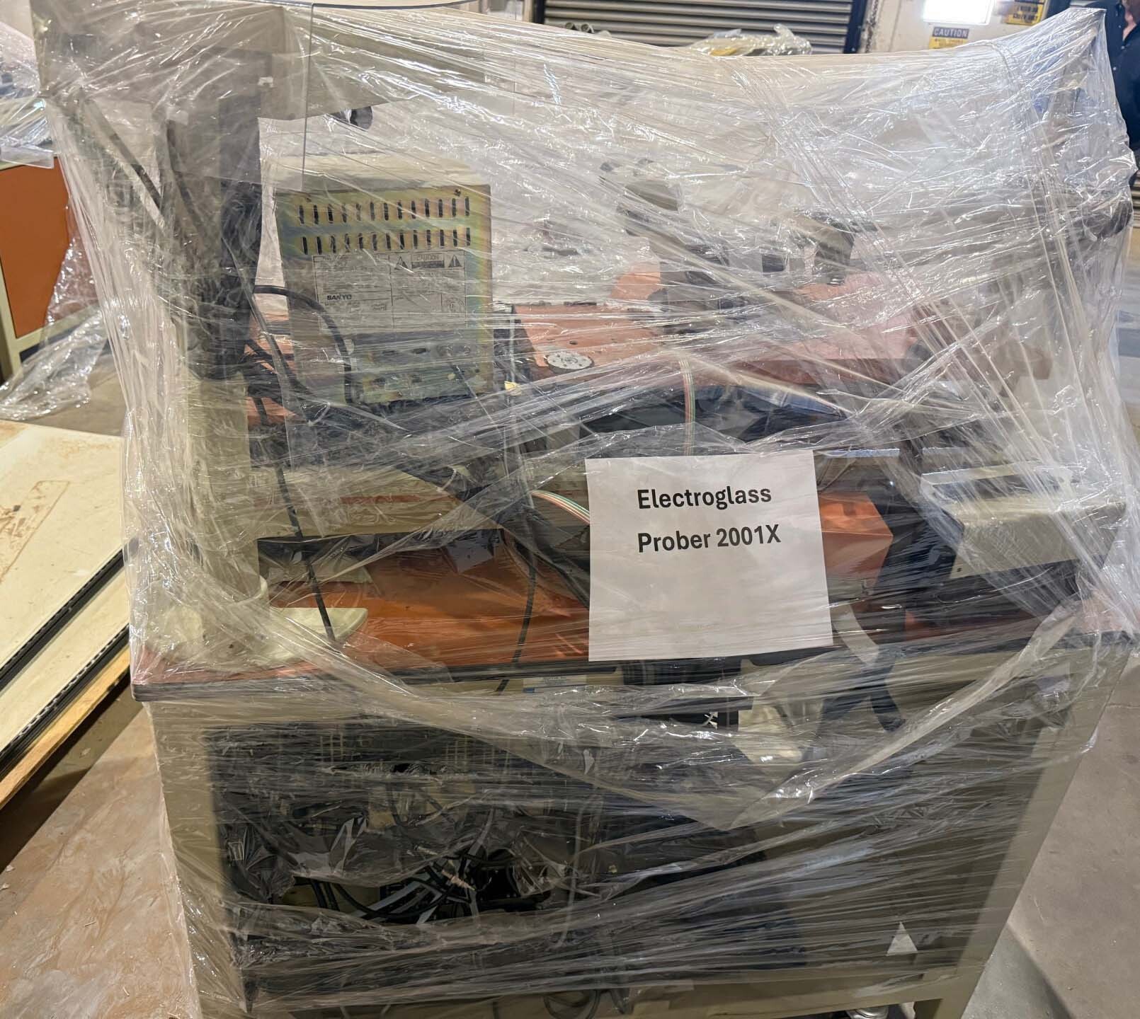
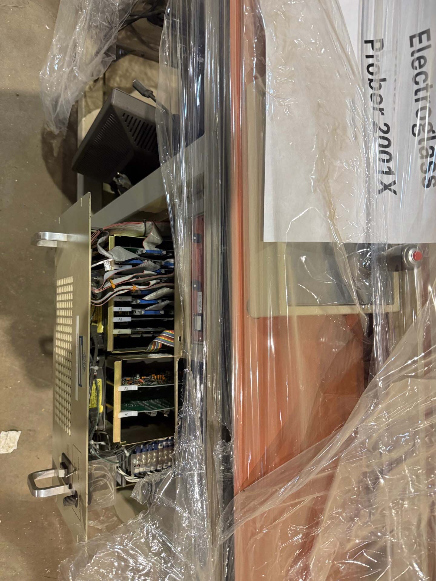
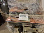
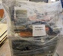
ELECTROGLAS / EG 2001CX is a prober designed to accurately measure and inspect the size and shape of integrated circuits on the nanometer scale. It features an XYZ interferometer that can measure points on a wafer within a range of 0.1 to 0.4 µm accuracy. It is optimized for both low cost of ownership and low-volume wafer probing run rates. The prober has a powerful and fast vector-based autofocus system for precise repeatability. Its automated wafer recognizer and autodetect features allow for fast automation and prober startup. EG 2001CX supports a maximum wafer diameter of up to 200mm, making it an excellent choice for inspected area-limited designs. The prober can accurately measure parameters such as feature size, line width, surface placement, critical dimension, and fine detailed patterns. The prober can be used to detect and measure small defects on the nanometer scale, and can be used to check any changes in the dimensions of the circuits. An advanced surface inspection module is available for the prober, allowing for a full range of 3D roughness maps. The prober features a high-speed parameter acquisition system that can sample up to 8 locations per second. This enables a rapid scan of the surface and movement between multiple X-Y locations without sacrificing accuracy. It is equipped with several automated prober features, such as wafer alignment, displacement table alignment, die-oriented substrate separation, and automatic tipdown. The data analysis algorithms integrated into the prober allows for real-time graphical data representation, making it possible for fast and accurate data interpretation. ELECTROGLAS 2001 CX prober is a reliable and cost-effective solution for measuring, inspecting, and analyzing integrated circuits. Its versatile features make it versatile and suitable for diverse applications. It is an excellent choice for both batch-mode and large-scale production.
There are no reviews yet