Used ELECTROGLAS / EG 4080 #293827239 for sale
URL successfully copied!
Tap to zoom
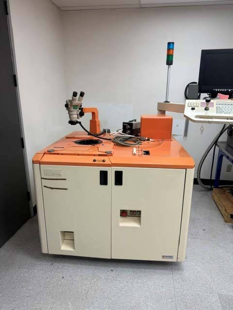

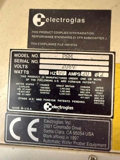
ELECTROGLAS / EG 4080 is a sophisticated and highly advanced semiconductor wafer prober designed for precise and efficient testing of semiconductor devices. This prober is an essential tool in the semiconductor manufacturing process, as it allows for accurate electrical testing of integrated circuits (ICs) on wafers before they are diced and packaged. EG 4080 prober is renowned for its high-performance capabilities, reliability, and ease of use, making it a popular choice among semiconductor manufacturers worldwide. It is equipped with state-of-the-art technology and features that enable it to handle a wide range of test requirements for various semiconductor devices. One of the key features of ELECTROGLAS EG4080 prober is its advanced probing capability, which allows for precise and repeatable contact between the test probe needles and the IC pads on the wafer. This ensures accurate and reliable electrical measurements, minimizing the risk of false readings or errors during testing. The prober is equipped with a high-precision alignment system that enables it to accurately position the test probes with respect to the IC pads on the wafer. This alignment system utilizes advanced vision systems and algorithms to achieve sub-micron accuracy, ensuring optimal contact and reliable test results. ELECTROGLAS / EG EG4080 prober also features a sophisticated chuck design that provides excellent thermal stability and uniformity during testing. This helps to minimize thermal effects and ensure consistent electrical measurements across the wafer, even when operating at high speeds or in demanding test conditions. In addition to its probing and chuck capabilities, the prober is equipped with a comprehensive software interface that allows users to easily program and control the testing process. The software provides intuitive tools for setting up test sequences, configuring test parameters, and analyzing test results, making it easy for operators to perform complex testing procedures with minimal training. ELECTROGLAS 4080 prober is designed to accommodate wafers of various sizes, from small-diameter wafers used in research and development to large-diameter production wafers. It can be configured with multiple test heads and probing cards to support high-throughput testing of multiple ICs simultaneously, increasing productivity and reducing test time. Overall, EG4080 prober is a versatile and reliable tool that meets the demanding requirements of semiconductor manufacturers for testing advanced semiconductor devices. Its advanced technology, precision probing capabilities, thermal stability, and user-friendly software interface make it an essential asset in the semiconductor industry for ensuring the quality and reliability of semiconductor devices.
There are no reviews yet