Used ELECTROGLAS / EG 4090 PSM #293821804 for sale
URL successfully copied!
Tap to zoom
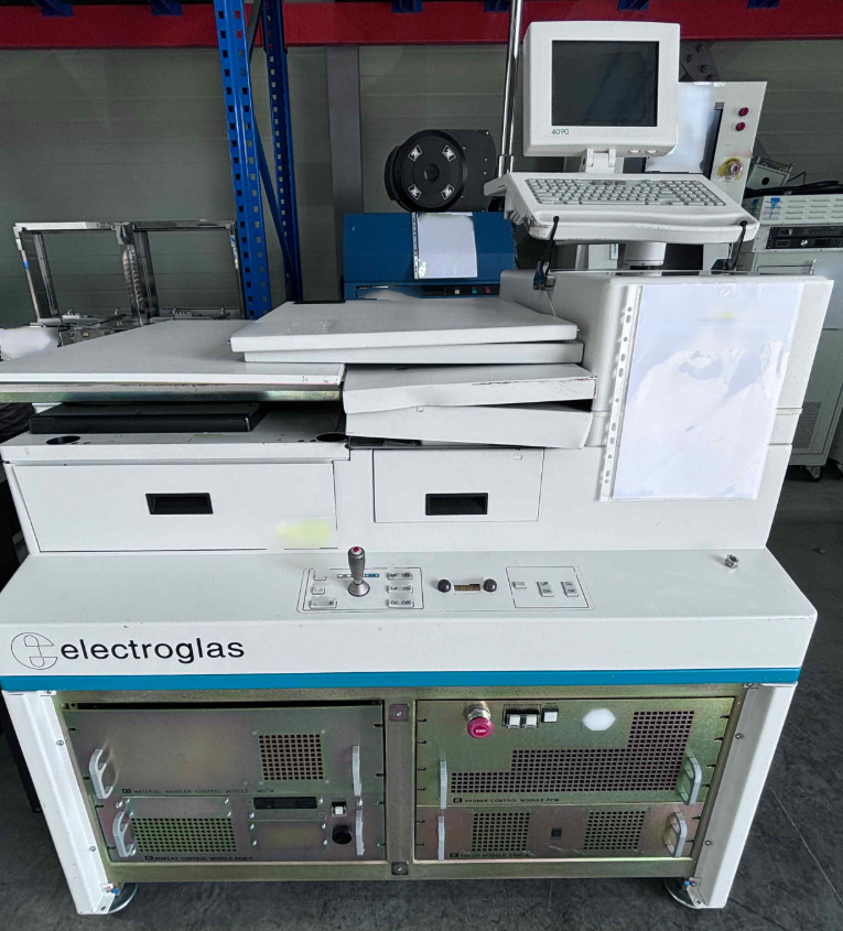

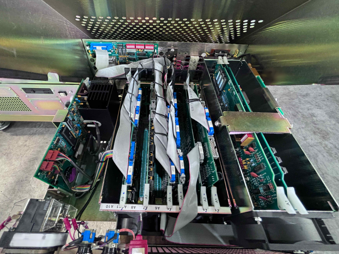
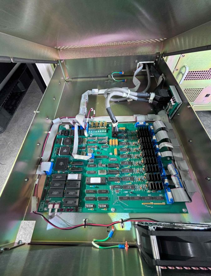
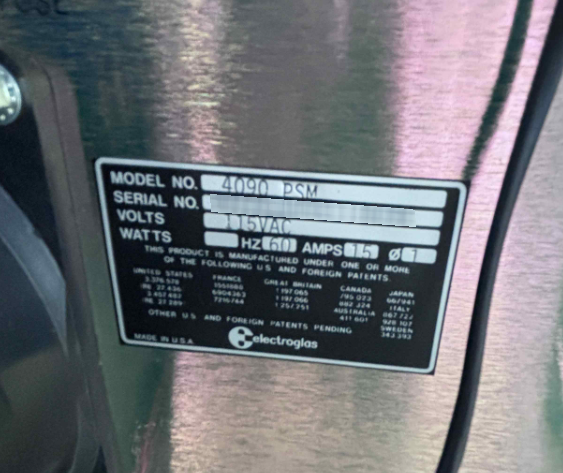
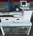
ELECTROGLAS / EG 4090 PSM is a powerful and high-precision automated wafer prober used in semiconductor manufacturing for testing integrated circuits (ICs) on silicon wafers. This prober is designed to handle wafers with diameters of up to 300mm and offers advanced features and capabilities that make it an essential tool for semiconductor testing and characterization. The key components of EG 4090 PSM include a precision stage manipulator, a probing mechanism, and a sophisticated control system. The stage manipulator is responsible for accurately positioning the wafer under the probing mechanism, ensuring precise alignment and contact with the test pads on the ICs. The probing mechanism consists of a set of high-performance probes that make electrical contact with the ICs on the wafer, allowing for the measurement of various electrical parameters such as resistance, capacitance, and inductance. One of the standout features of ELECTROGLAS 4090 PSM is its advanced automation capabilities. The prober is equipped with a robotic wafer handling system that can load and unload wafers automatically, reducing the need for manual intervention and increasing throughput. Additionally, the prober can be integrated with software systems for test program generation, data analysis, and reporting, streamlining the testing process and enhancing overall efficiency. 4090 PSM also offers superior performance in terms of accuracy and repeatability. The prober is equipped with high-precision stages and probes that ensure consistent and reliable measurement results, even for small and densely packed ICs. The prober's control system is capable of adjusting probe force, position, and other parameters in real-time, optimizing the contact between the probes and the ICs and minimizing the risk of damage to the wafer. In addition to its performance and automation features, ELECTROGLAS / EG 4090 PSM is known for its versatility and flexibility. The prober is compatible with a wide range of test configurations and can be easily customized to accommodate different wafer sizes, probe types, and test requirements. This flexibility makes the prober suitable for a variety of applications, including parametric testing, failure analysis, and device characterization. Overall, EG 4090 PSM is a sophisticated and reliable wafer prober that plays a crucial role in semiconductor testing and quality assurance. Its advanced automation capabilities, precision measurement performance, and versatility make it an indispensable tool for semiconductor manufacturers looking to ensure the reliability and functionality of their ICs. With its cutting-edge technology and robust design, ELECTROGLAS 4090 PSM sets the standard for automated wafer probing in the semiconductor industry.
There are no reviews yet