Used ELECTROGLAS / EG 4090 #293751159 for sale
URL successfully copied!
Tap to zoom

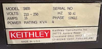
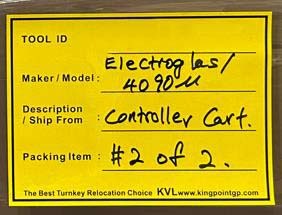
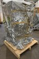
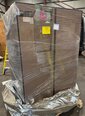
ELECTROGLAS 4090 prober is an automated wafer prober used for testing the electrical properties of semiconductor wafers. Its advanced design and capabilities make it ideal for high volume production lines and laboratories. 4090 prober is designed to be fast, accurate and repeatable. Its advanced motion systems provide precision piezo-driven alignment, with linear and rotational motion to the nanometer scale. Its high-speed laser scanning system quickly aligns to probe cards, ensuring contact is made within seconds. ELECTROGLAS 4090 prober can handle a variety of wafer sizes and shapes and can accommodate up to four probe cards at a time. In addition, it has galvanometer scanners and automated heat transfer systems that allow it to quickly and accurately conform to direct connection testing. The prober is powered by a Windows-based PC that allows external programs to interface with the machine. 4090 prober is also equipped with an integrated vision system that helps improve accuracy and alignment, as well as providing remote probing and vectoring capabilities. In addition to its physical design, ELECTROGLAS 4090 prober is equipped with advanced control features. These features enable users to set up individual tests and instructions, customize parameters, and program more complex test specifications. It also features two different auto-alignment modes, allowing for either manual stepping or dedicated pattern recognition. Its analyzer system is capable of high-response voltage and current measurements, as well as automated DC testing. 4090 prober is designed to exceed industry standards, providing optimal accuracy and repeatability of results. It is capable of handling large wafer sizes, high throughputs, and complex testing requirements. It is an ideal tool for testing electrical circuits, semiconductor devices, and other components.
There are no reviews yet