Used ELECTROGLAS / EG 4090µ #293753146 for sale
URL successfully copied!
Tap to zoom
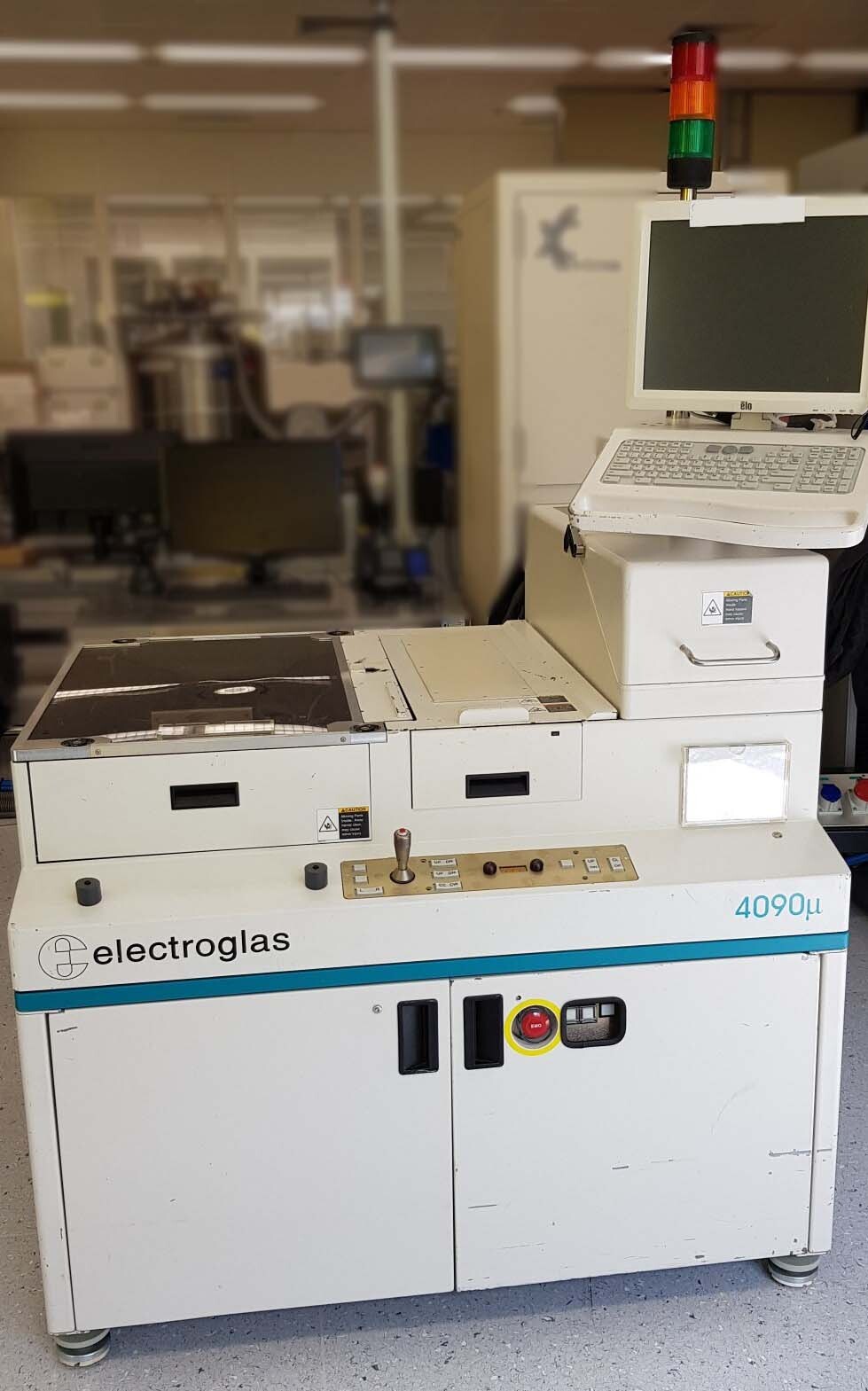

ELECTROGLAS / EG 4090µ is a high-precision fully automatic wafer prober designed for semiconductor testing applications. This advanced prober offers cutting-edge technology and features to facilitate efficient and accurate testing of semiconductor wafers, making it a preferred choice for semiconductor manufacturers and testing facilities. At the core of EG 4090µ prober is its innovative mechanical design, which enables precise and repeatable positioning of wafers for testing. The prober is equipped with a sophisticated motion control system that allows for micron-level positioning accuracy, essential for probing small semiconductor devices with tight tolerances. The prober's robust construction ensures stability and rigidity, minimizing vibrations and any external disturbances that could affect testing results. One of the key features of ELECTROGLAS 4090µ prober is its versatile chuck design that accommodates various wafer sizes and types. The prober is capable of handling wafers ranging from 2 to 8 inches in diameter, offering flexibility to test different semiconductor devices on a single platform. The chuck design also incorporates proprietary technology to ensure efficient and reliable wafer handling during the testing process. Furthermore, 4090µ prober is equipped with advanced automation capabilities, allowing for fully automated wafer testing procedures. The prober can be seamlessly integrated into existing semiconductor testing workflows, streamlining the testing process and improving overall productivity. Automated features such as alignment, probing, and data collection enable rapid and accurate testing of semiconductor wafers, reducing testing time and increasing throughput. In addition to its precision and automation capabilities, ELECTROGLAS / EG 4090µ prober boasts an intuitive user interface that simplifies operation and enhances user experience. The prober is equipped with a user-friendly software interface that provides real-time monitoring of the testing process and allows for easy configuration of testing parameters. The software also offers advanced data analysis tools for in-depth analysis of testing results, facilitating quick decision-making and process optimization. Moreover, EG 4090µ prober integrates sophisticated probing technology to ensure reliable and accurate electrical contact between the prober needles and the semiconductor devices under test. The prober is equipped with high-performance probes and contactors that minimize signal loss and ensure consistent electrical contact during testing. This advanced probing technology contributes to the prober's high accuracy and repeatability, essential for achieving reliable testing results. Overall, ELECTROGLAS 4090µ prober stands out as a top-of-the-line solution for semiconductor testing applications, offering unmatched precision, automation, and user-friendly features. Its advanced capabilities make it an ideal choice for semiconductor manufacturers and testing facilities looking to improve testing efficiency, accuracy, and productivity. With its state-of-the-art technology and robust design, 4090µ prober sets a new standard for semiconductor testing equipment, enabling the precise and reliable testing of semiconductor devices for a wide range of applications.
There are no reviews yet