Used ELECTROGLAS / EG 4090u #293589335 for sale
URL successfully copied!
Tap to zoom
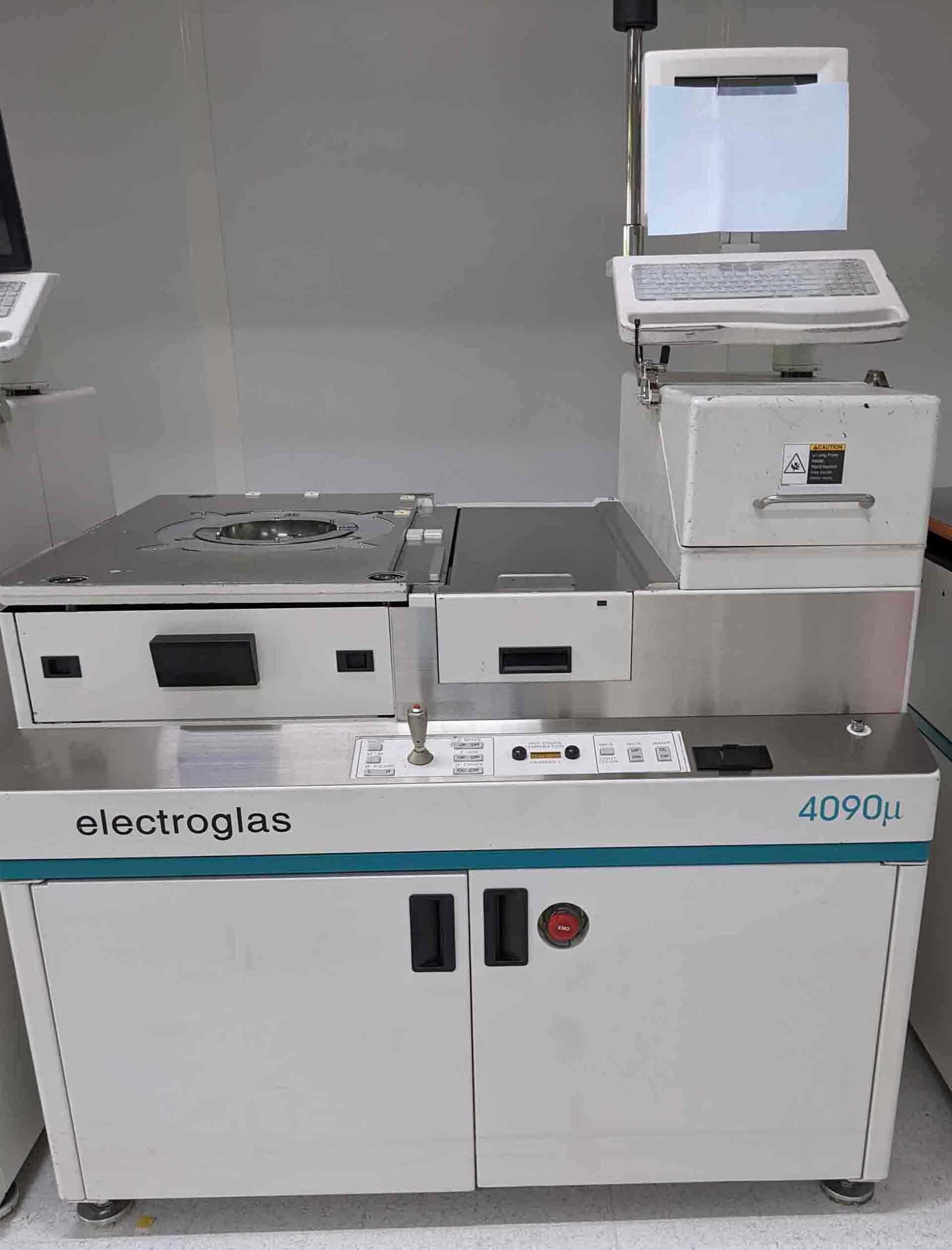






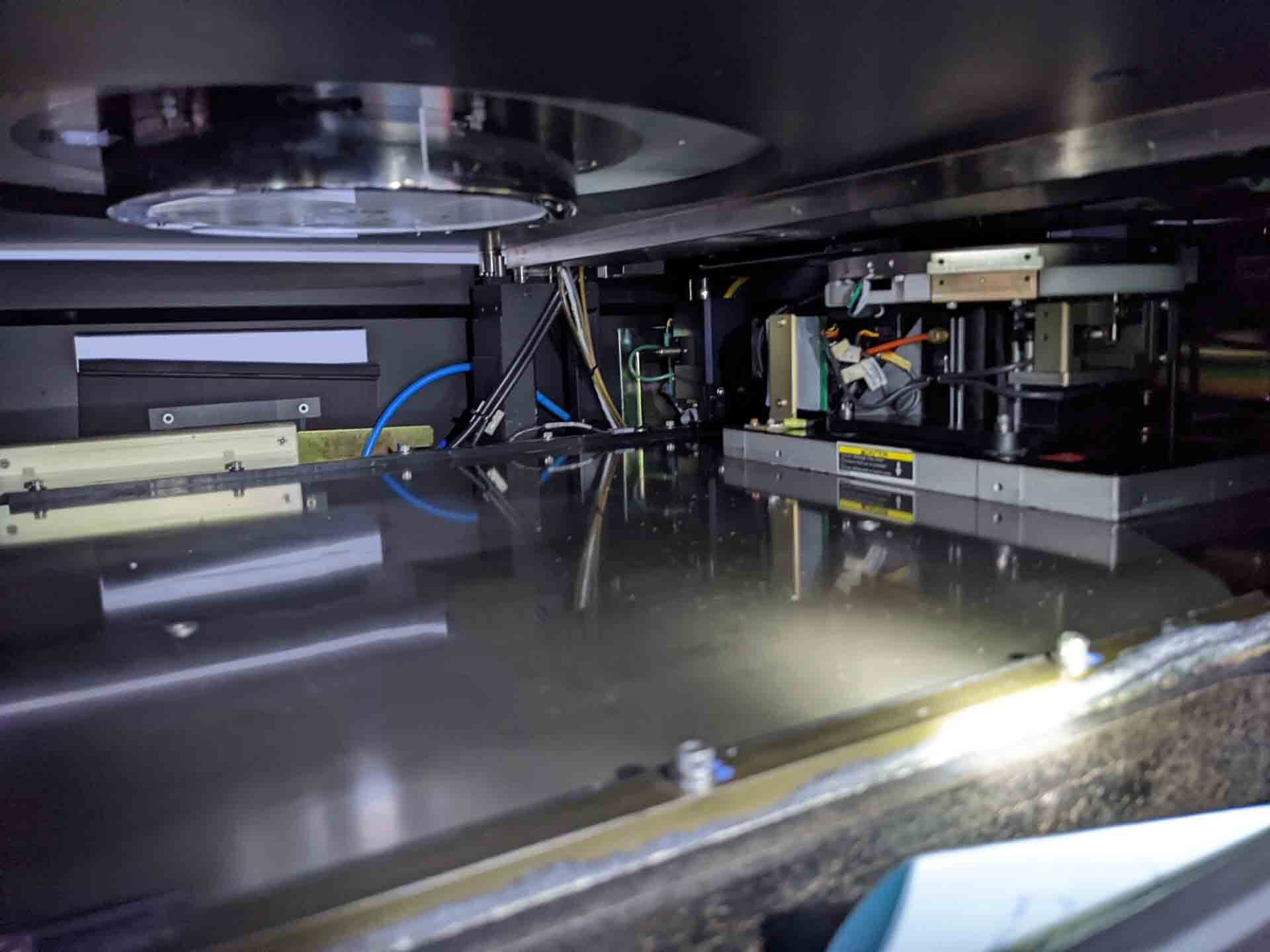

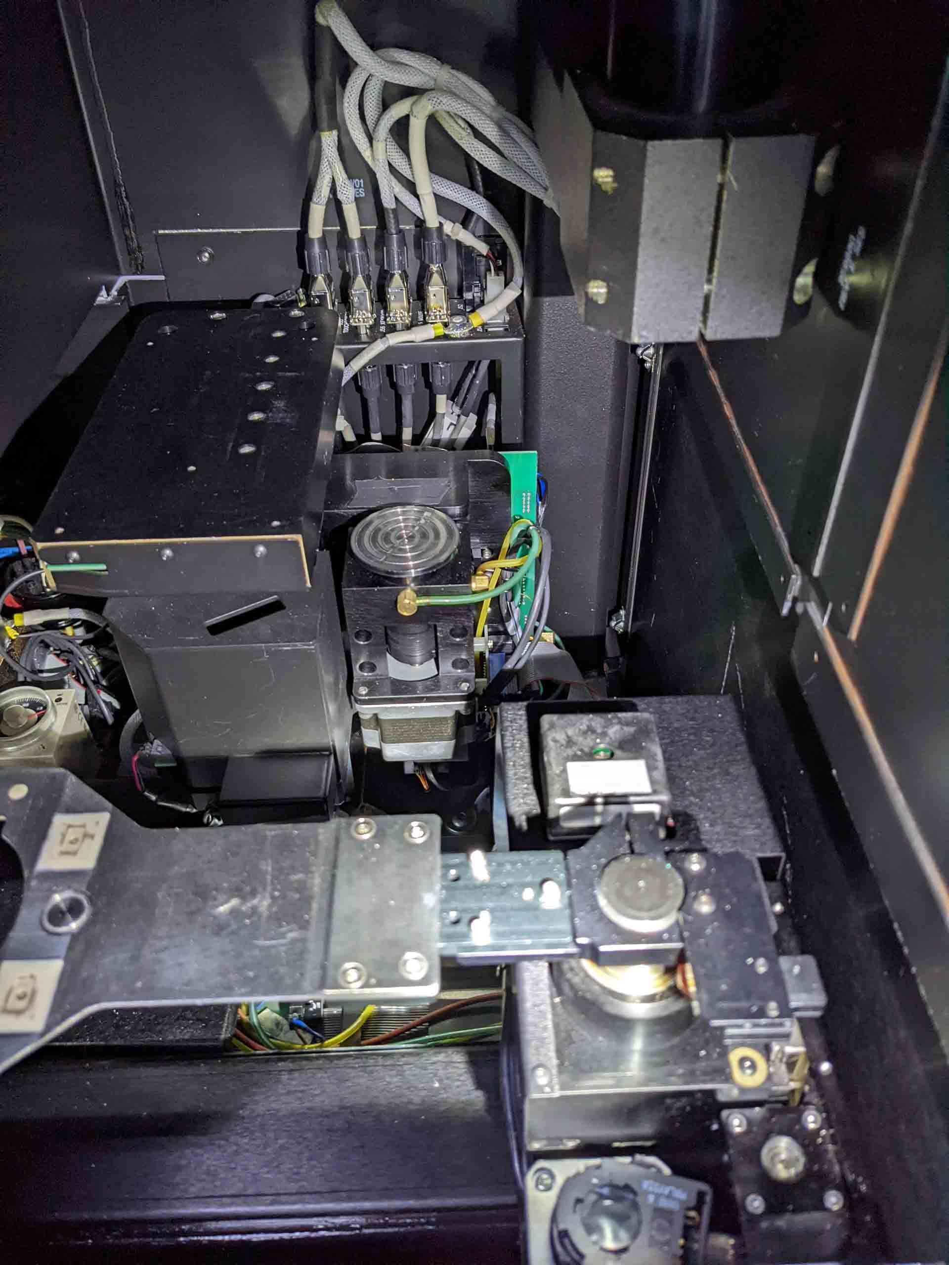

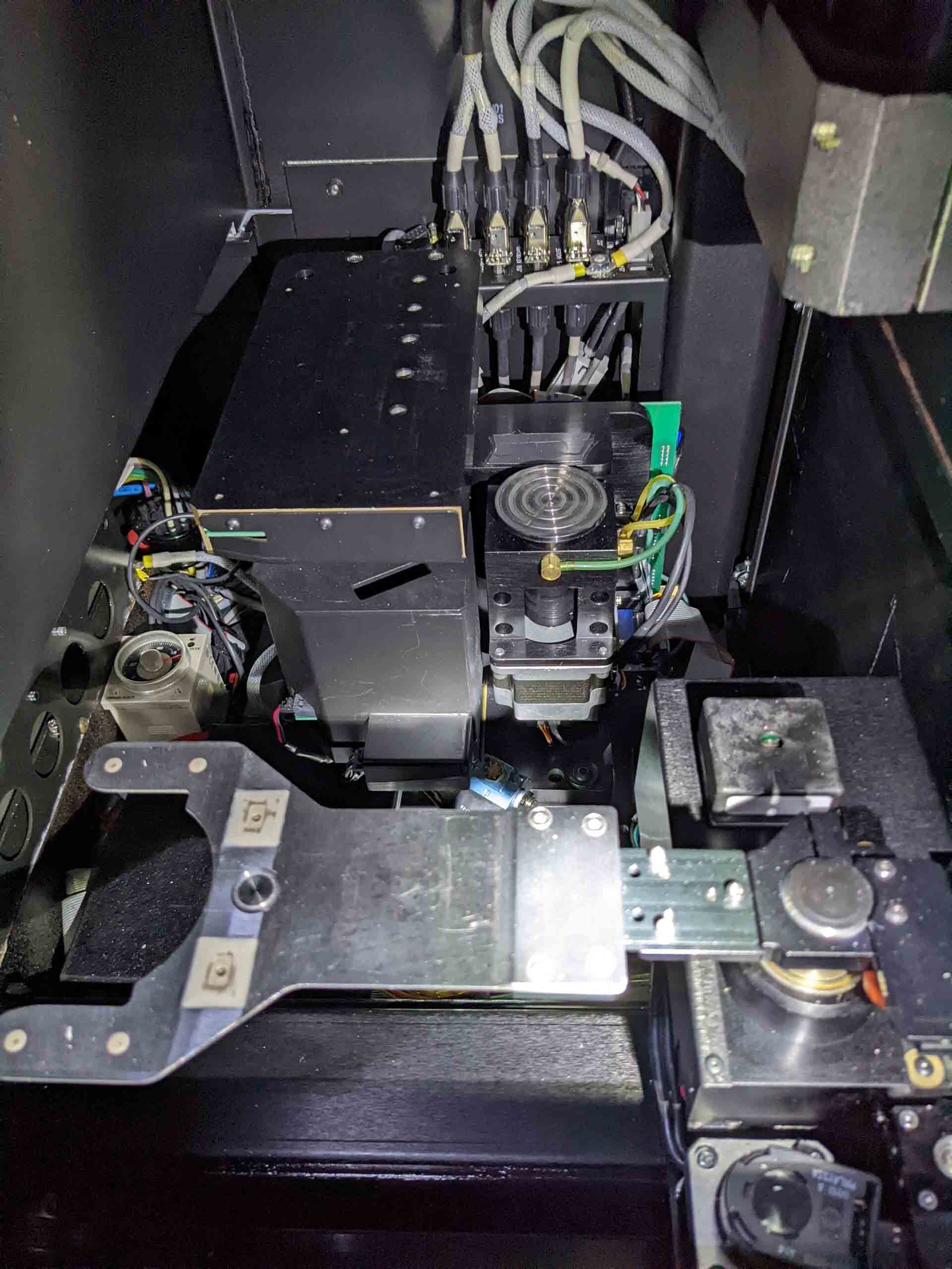


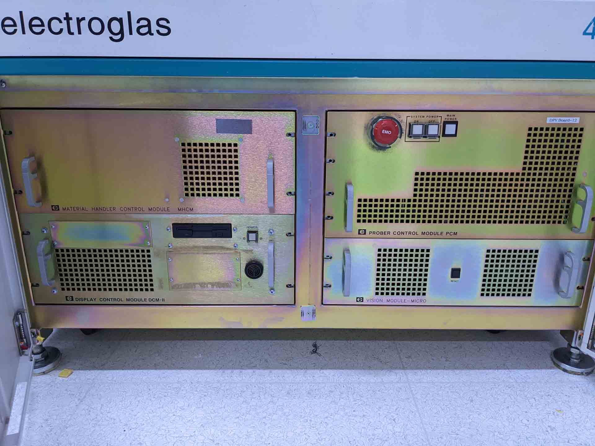

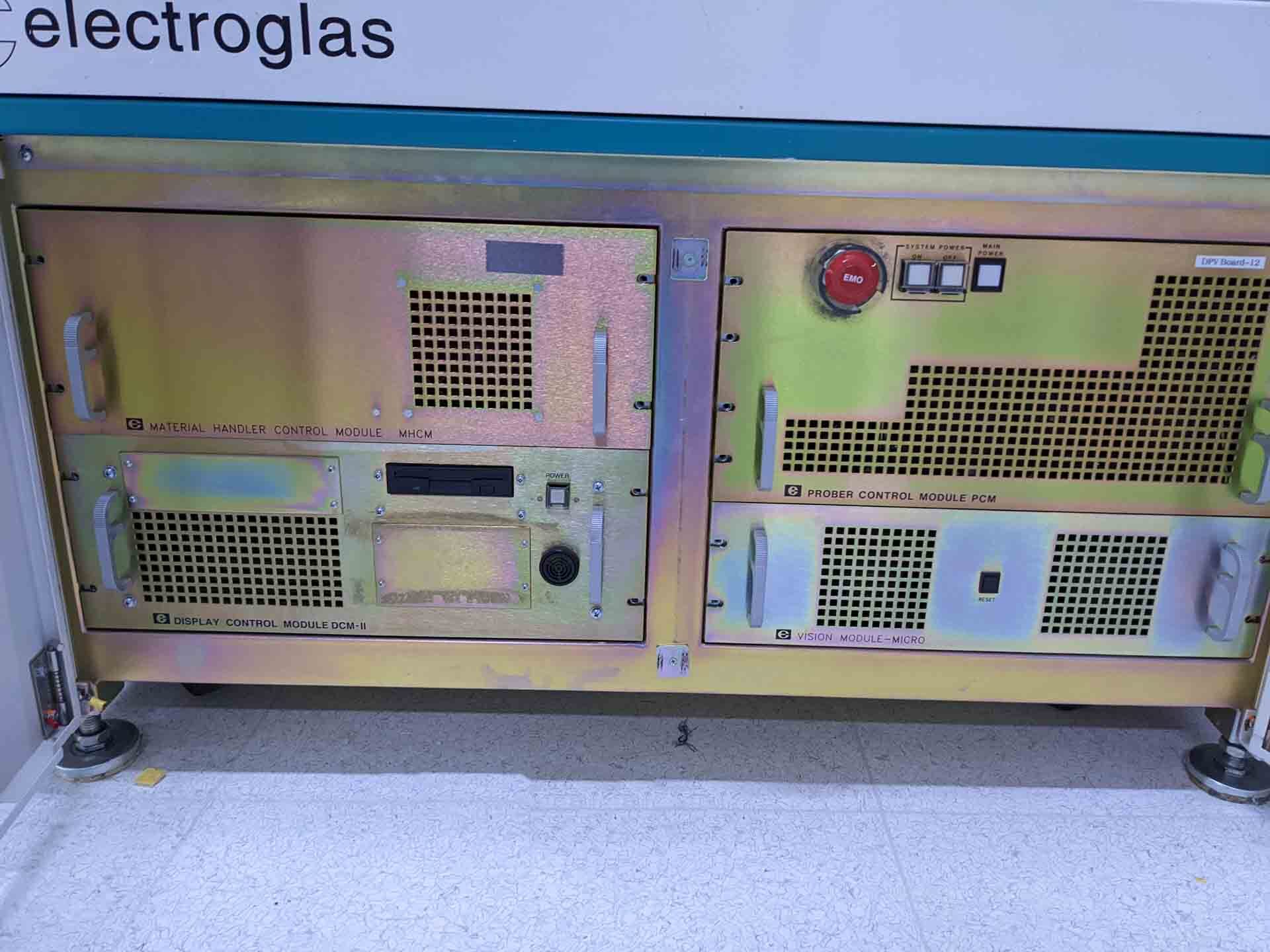

ID: 293589335
Vintage: 2000
Prober
Commander version: DOS EGC 7.3.8
DCM Version: DCM 2
Option: Thin wafer
VM Alignment system
Z-Stage: 0.125
Chuck material: Nickel
Chuck type: Hot
LCD Monitor
Material handler module
Display control module
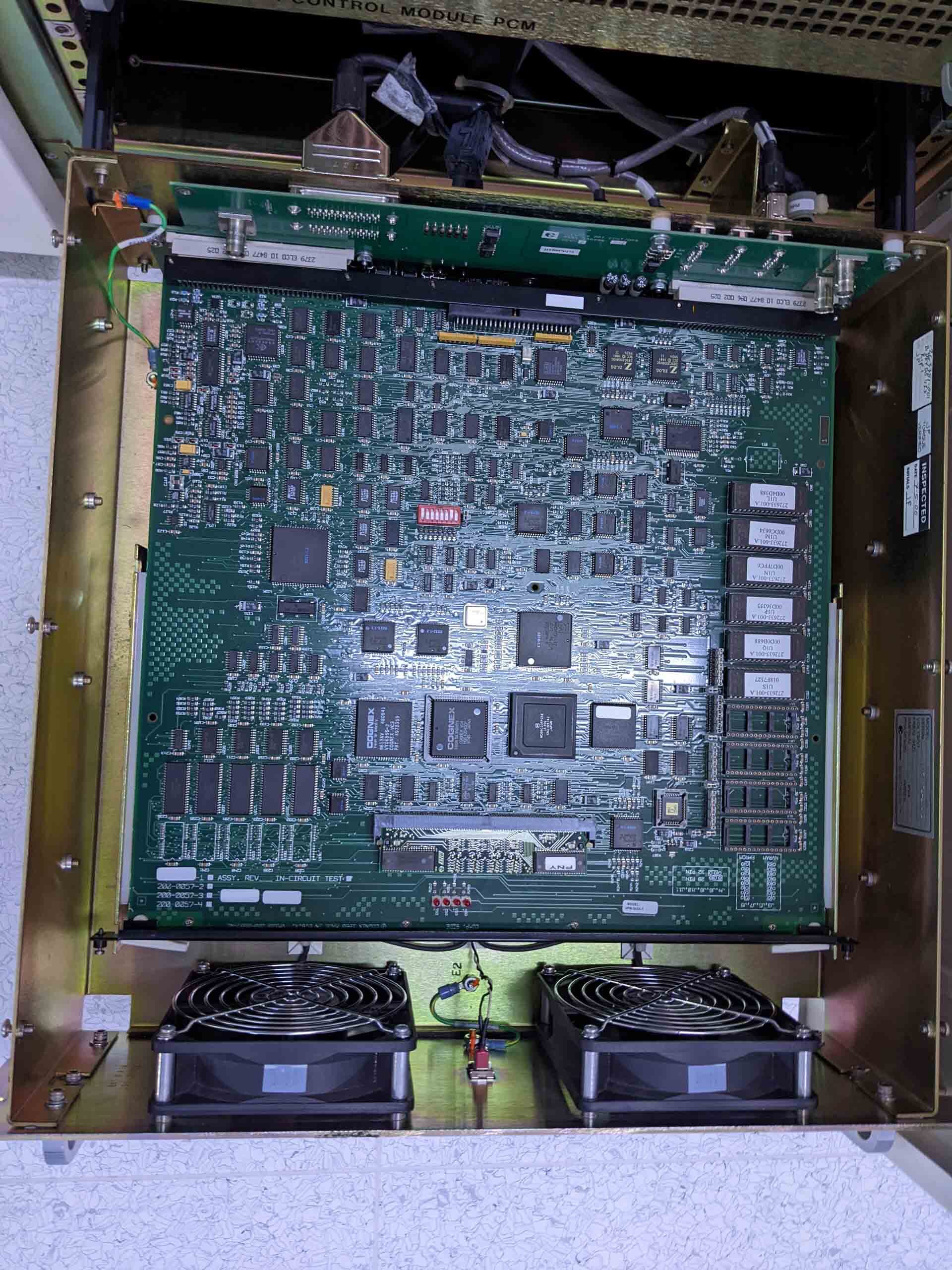
Prober control module
Vision module
OCR Camera
Bridge camera: COHU
2000 vintage.
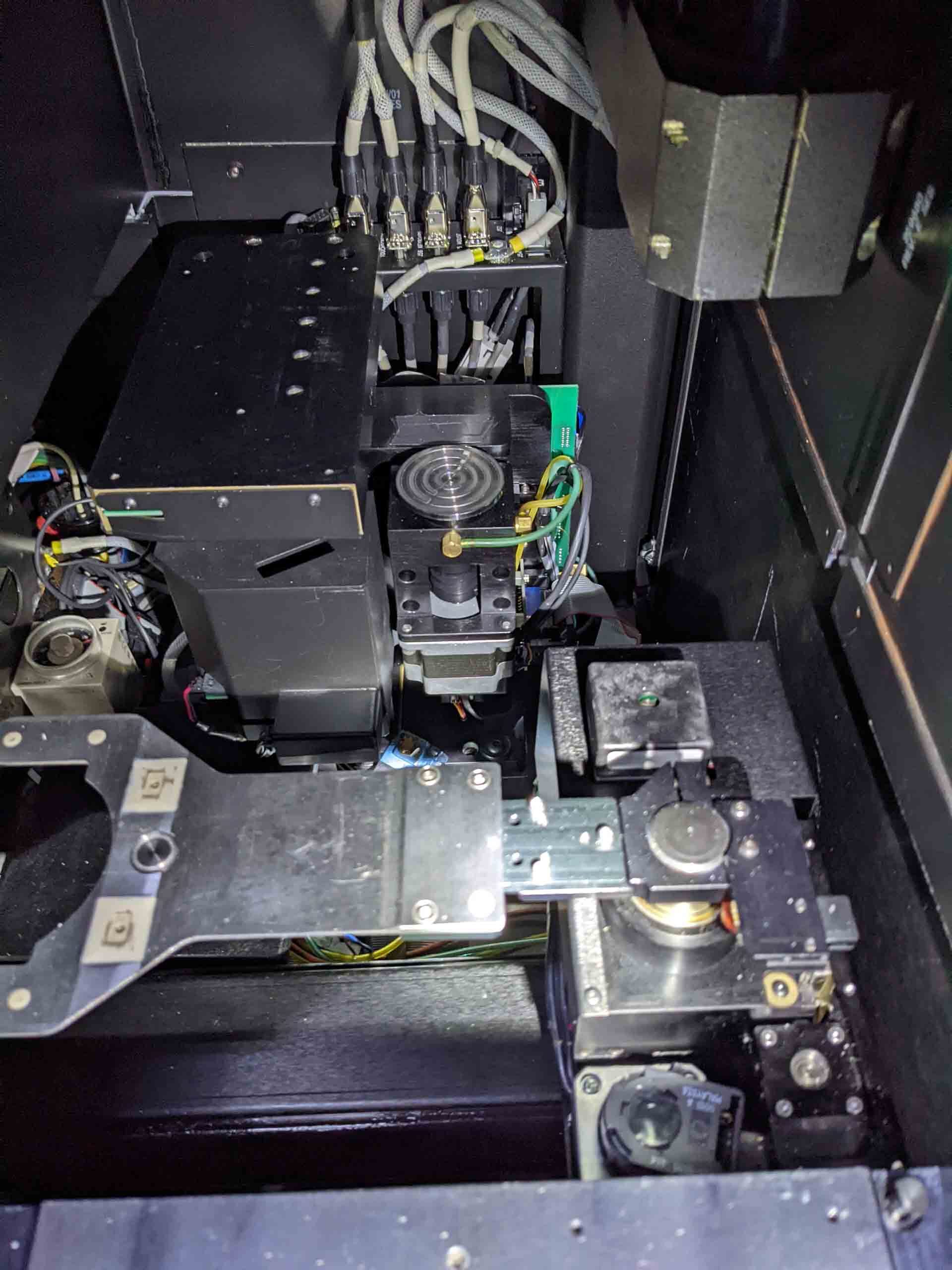
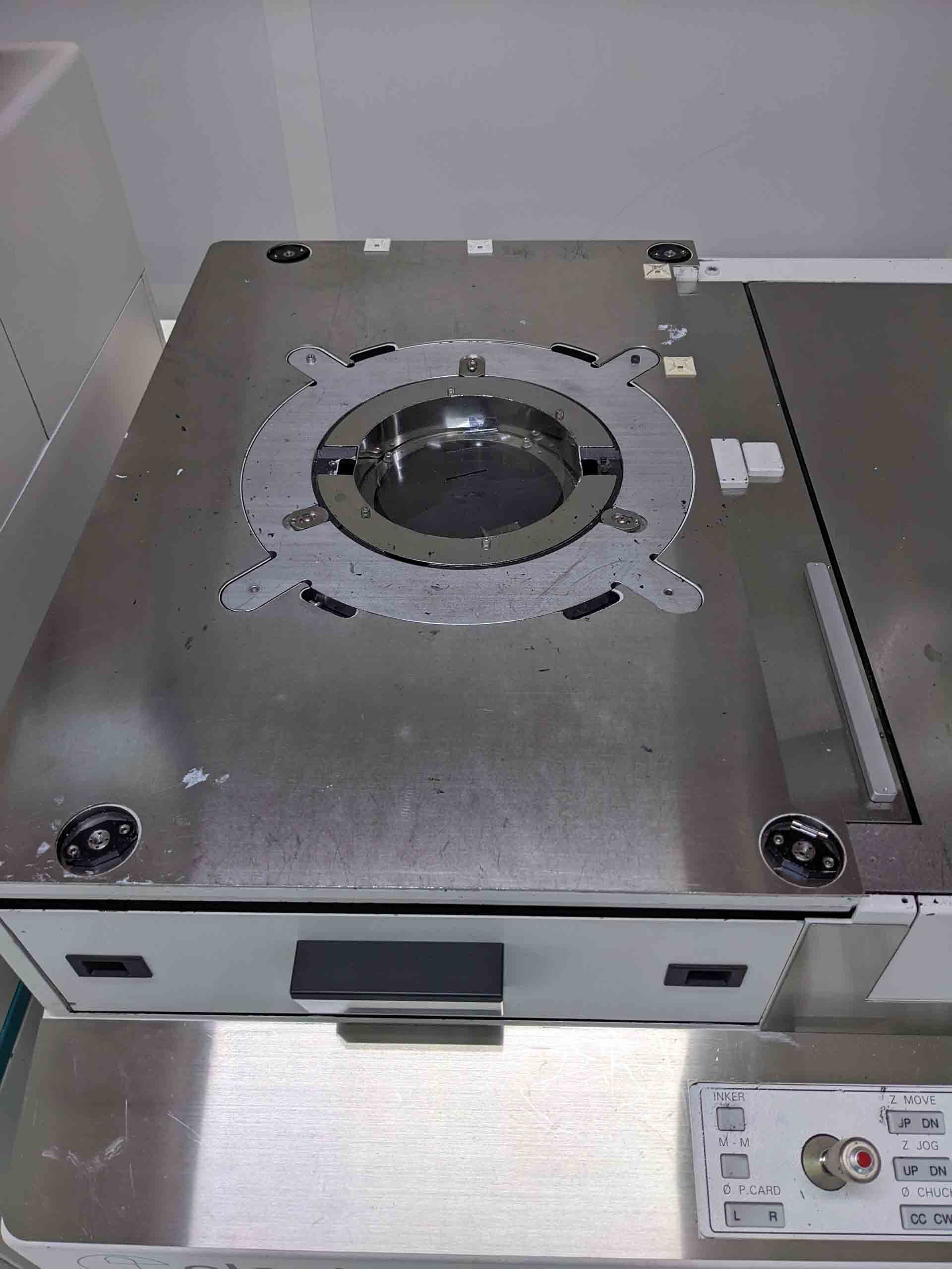
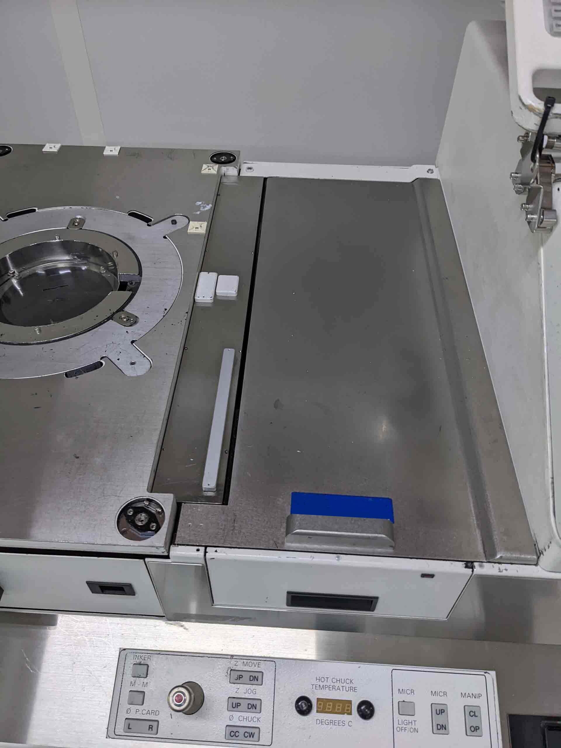
ELECTROGLAS / EG 4090u is a prober that automates the probing process of semiconductor devices. It is capable of providing rapid, precise, and automated wafer probing within a wide operating temperature range. The machine is designed for high-density probing and testing of various device architectures, providing high throughput, accurate alignment and transfer, and efficient handling of a wide range of semiconductor probes. With these features, EG 4090u delivers greater flexibility and yield in semiconductor production operations. The electromechanical equipment of ELECTROGLAS 4090 U is designed for both productivity and precision. It is equipped with a "slider" system and a motor-driven linear bearing, which supports high lateral accuracy and repeatability over a wide range of operating temperatures. In addition, the advanced control unit is designed to smooth out the dynamic response of mechanical processes, providing accurate fine alignment and translation even at high probing speeds. 4090 U also comes with a comprehensive set of advanced probing capabilities. The advanced contact algorithms allow for accurate, yet highly flexible and repeatable probing. Metrology Edge Probe technology provides new ways to test ultra-small features, such as micro-bumps and fine pitch pads on advanced nodes. In addition, the machine's integrated high-speed electrostatic chuck (ESC) allows for high temperature wafer handling without the use of additional vacuum systems. 4090u also offers touch-off capabilities for inspecting and probing ultra-low-profile components. The tool's advanced probing feature set includes touch-off probing, electrical stress testing, and scanning techniques, allowing users to precisely verify device characteristics. Moreover, the asset has an integrated vision model capable of accurately aligning, locating, and inspecting parts. In conclusion, EG 4090 U is a highly capable and versatile prober that offers sophisticated probing capabilities and reliable automation. It is designed to meet the extreme requirements of a wide range of semiconductor production operations, providing high-speed wafer probing, accurate alignment and transfer, and efficient handling of a variety of device architectures. The equipment is designed to provide a robust, cost-effective solution for pushing yields and speeding up production.
There are no reviews yet


