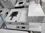
Used ELECTROGLAS / EG 4090u #293606395 for sale
URL successfully copied!
Tap to zoom
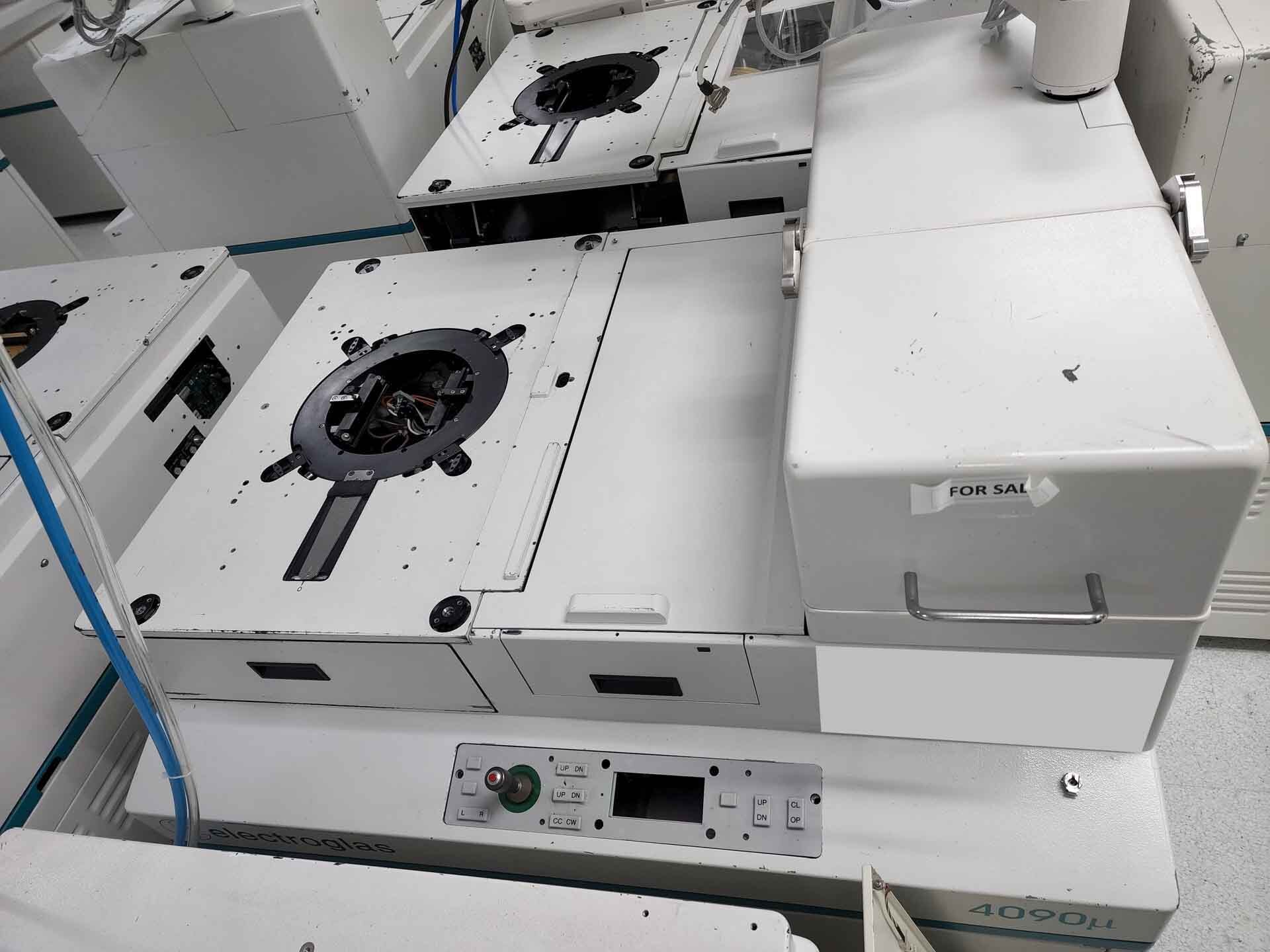


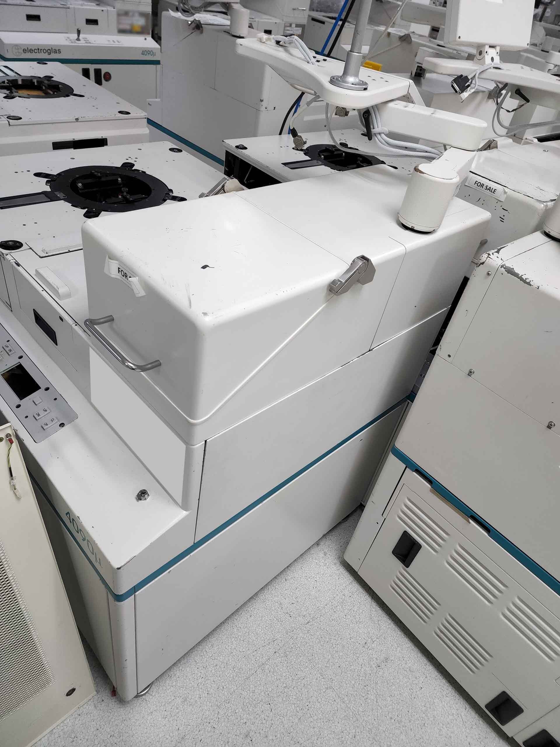





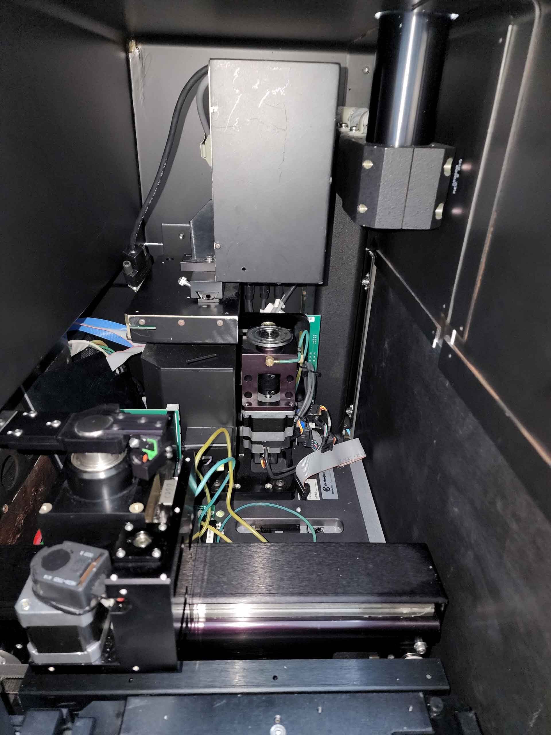

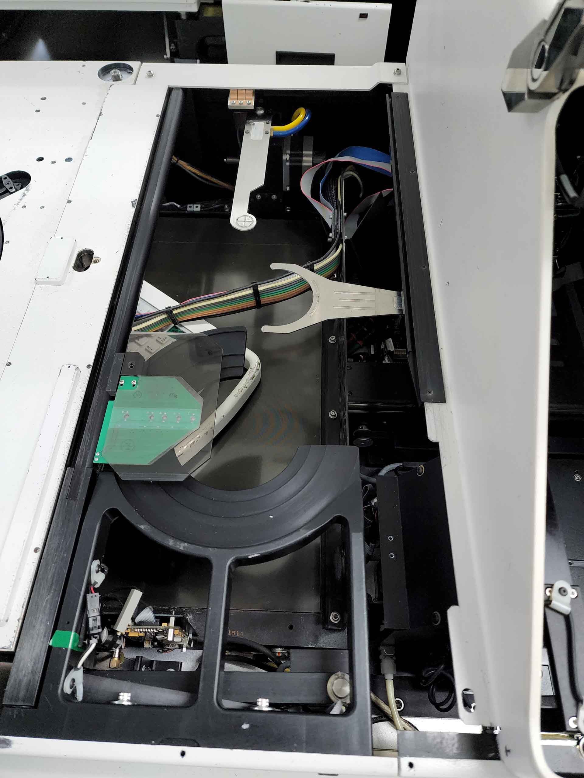

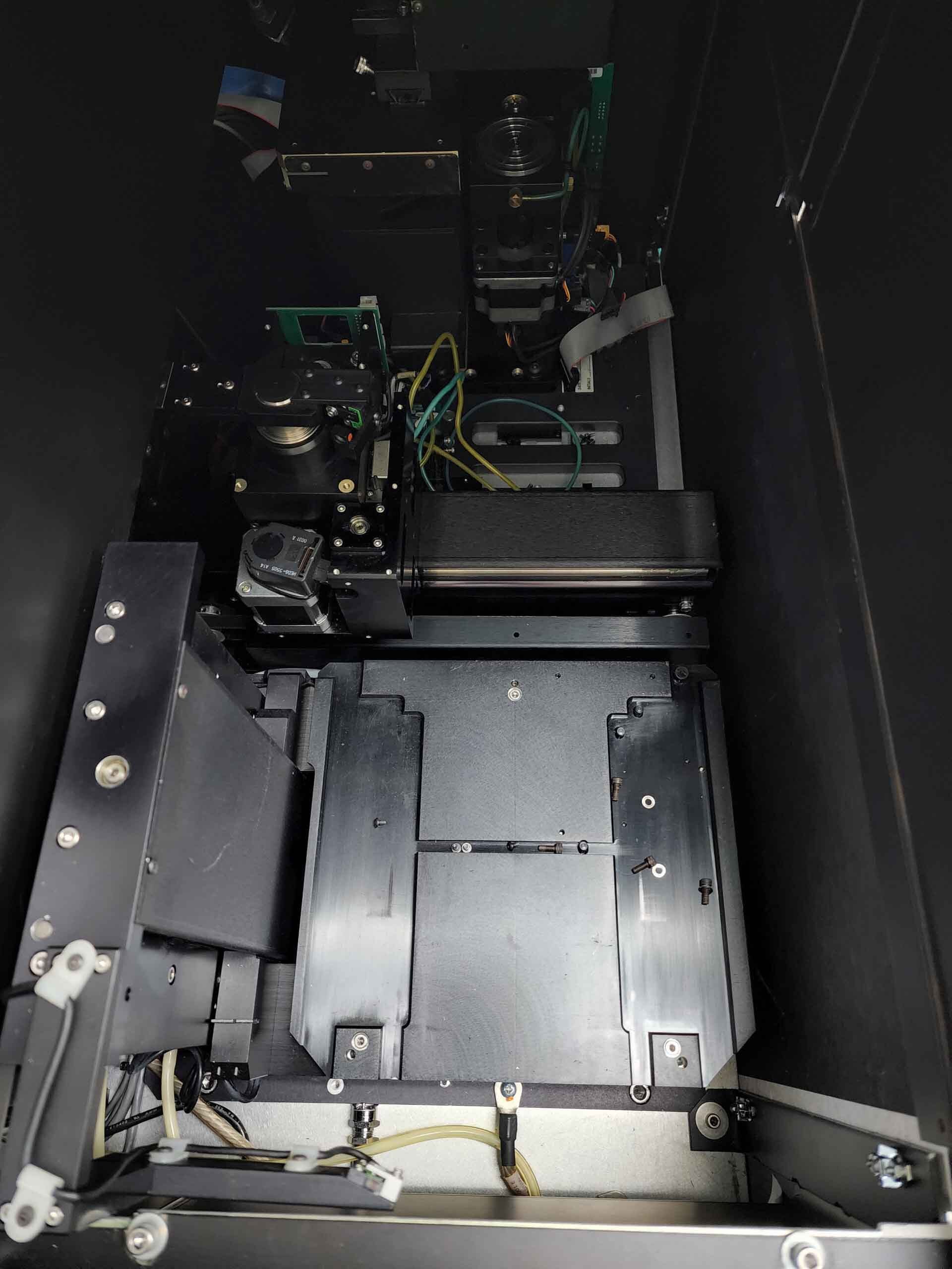

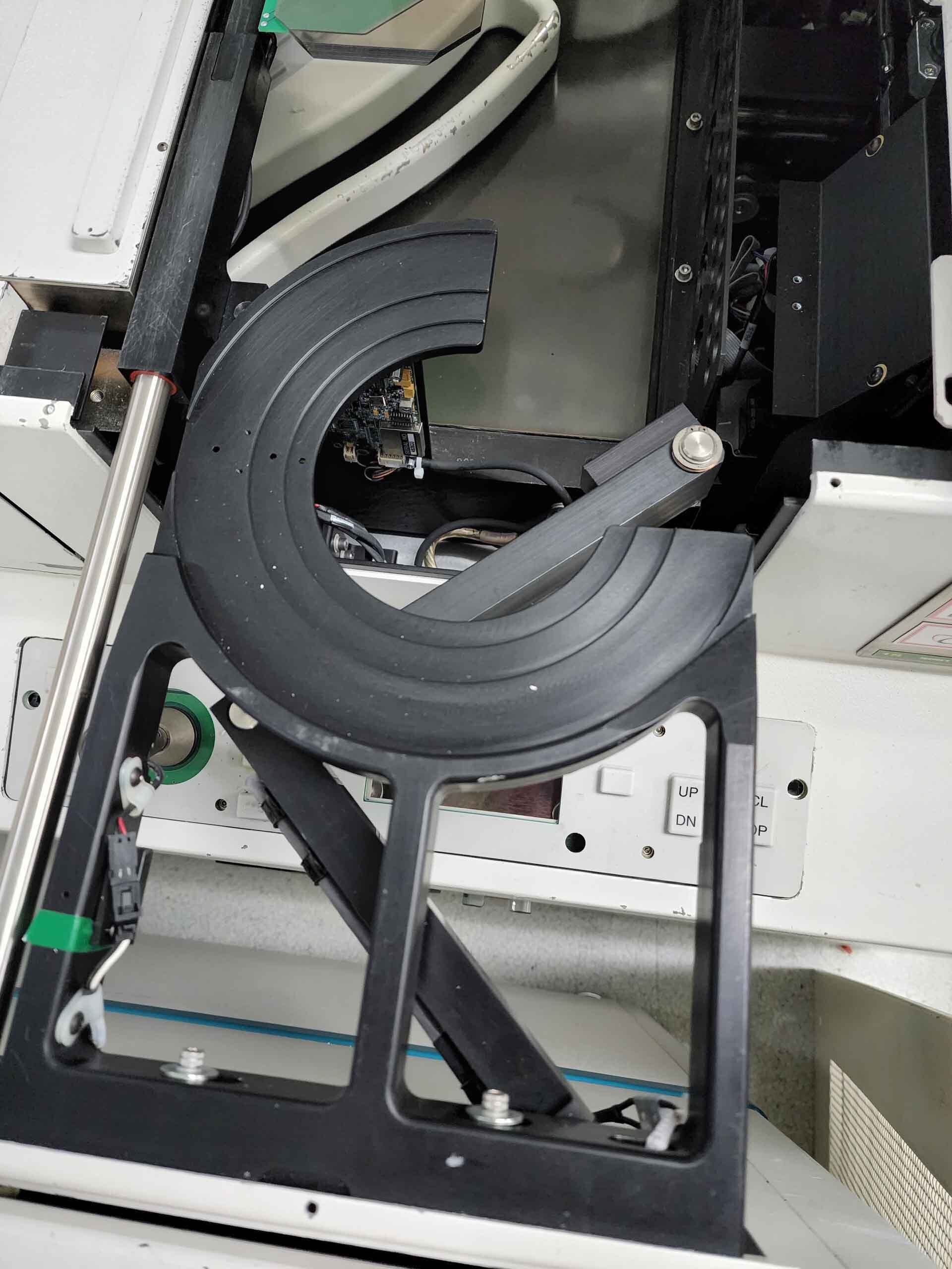

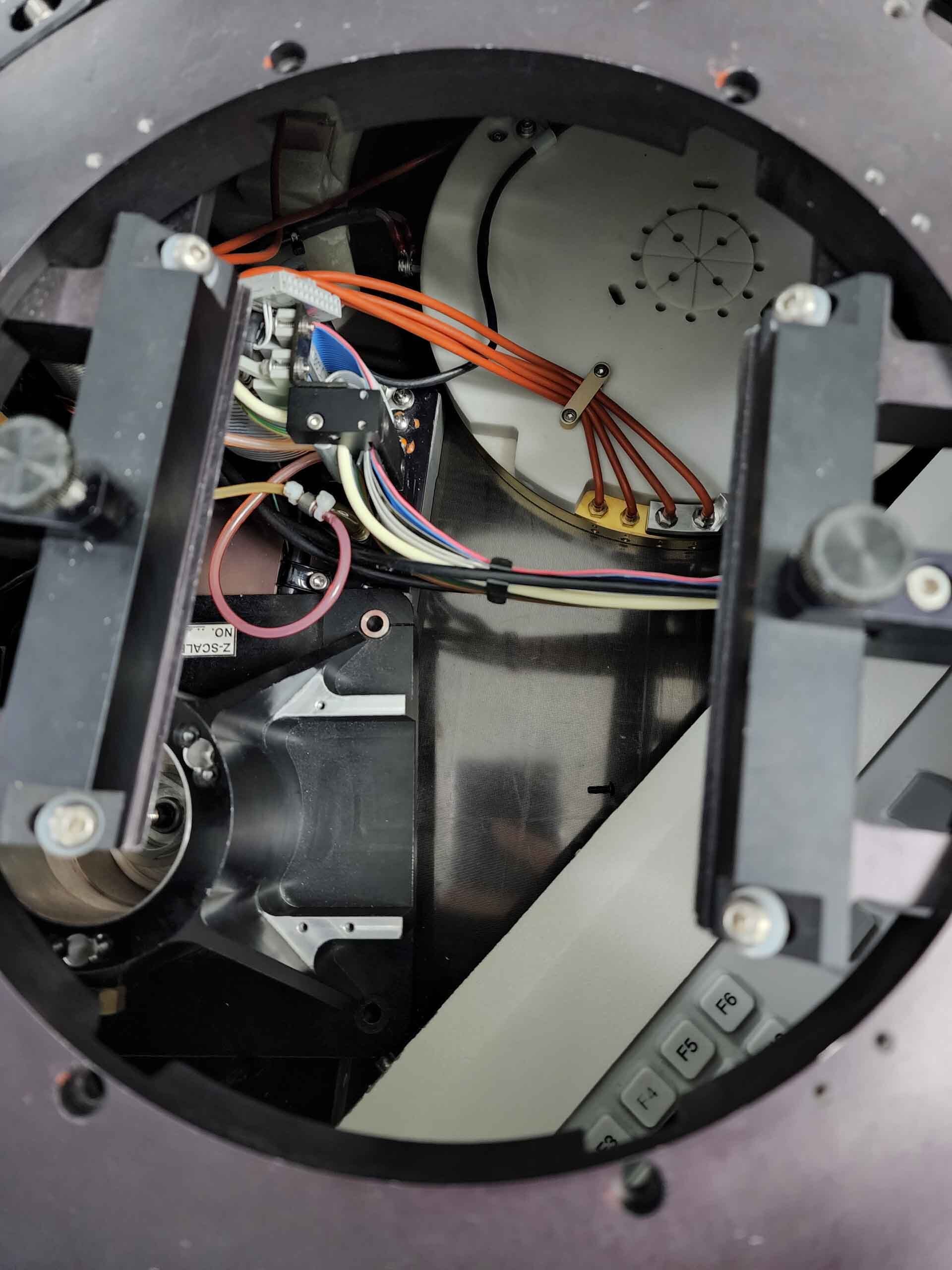

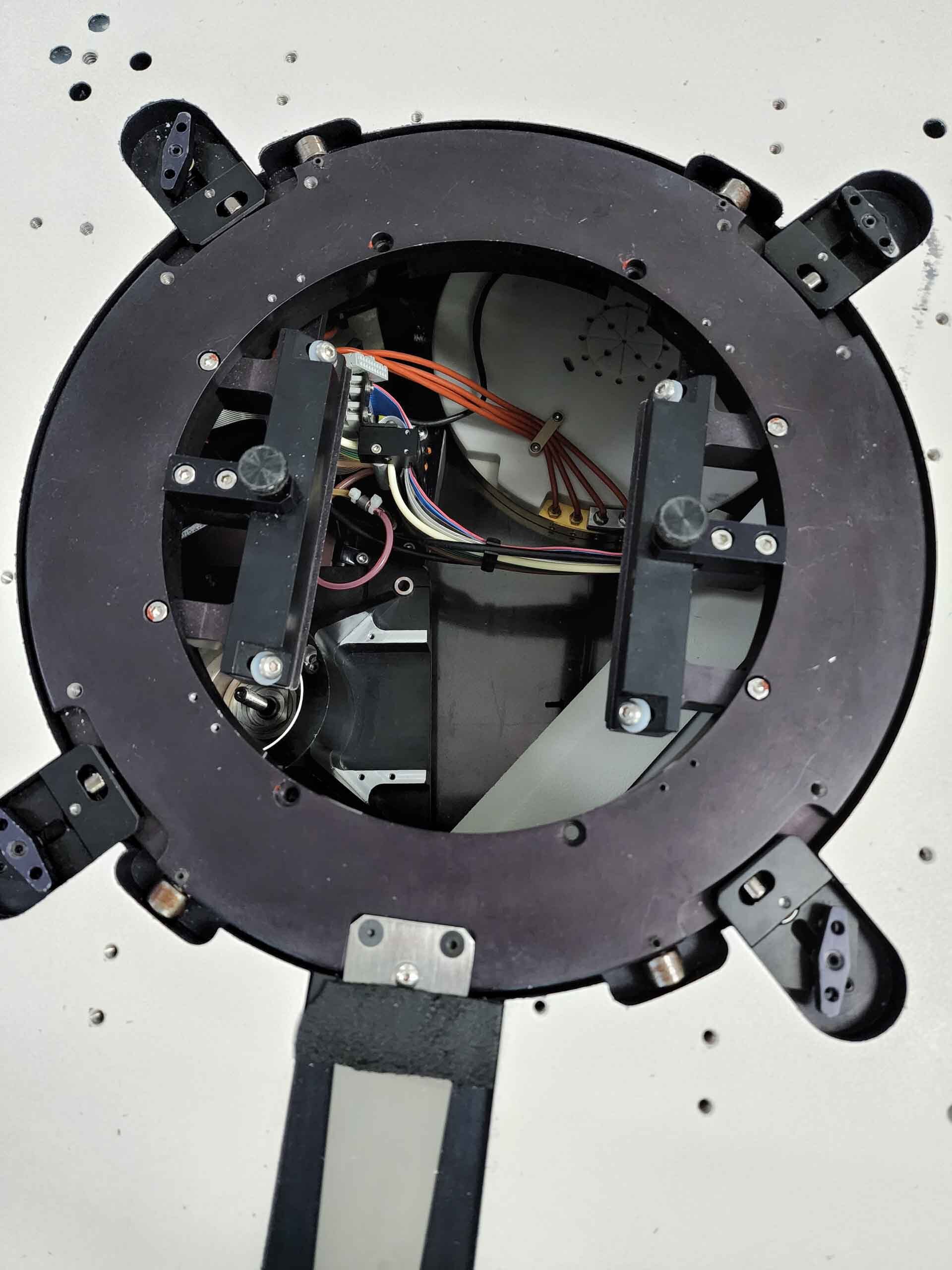

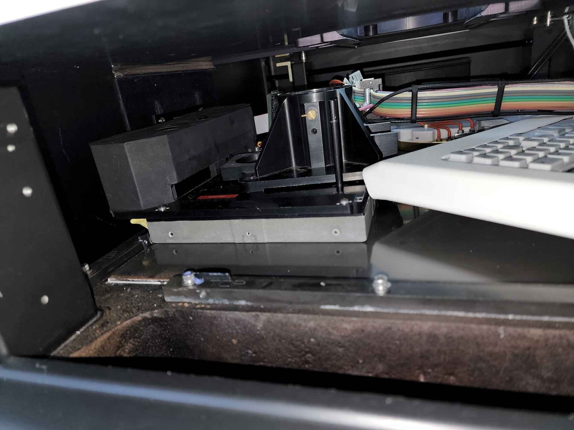

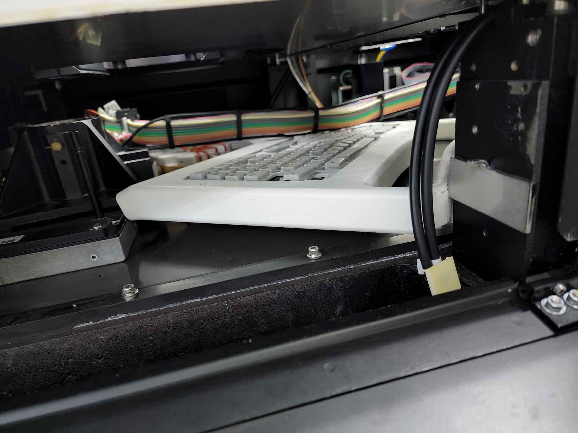




ID: 293606395
Wafer Size: 6"-8"
Wafer prober, 6"-8"
Standard chuck
Ambient temperature.
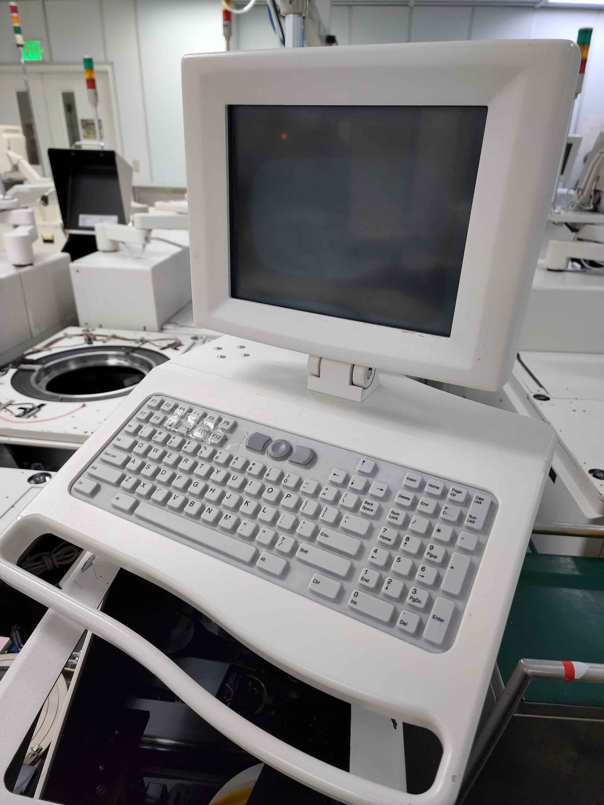
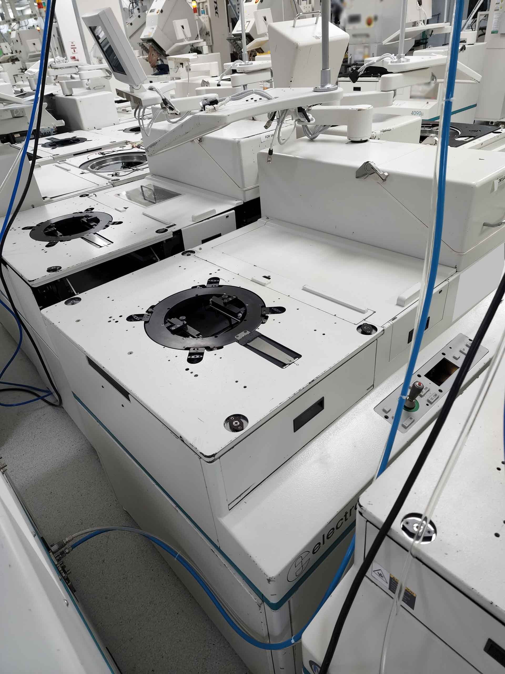
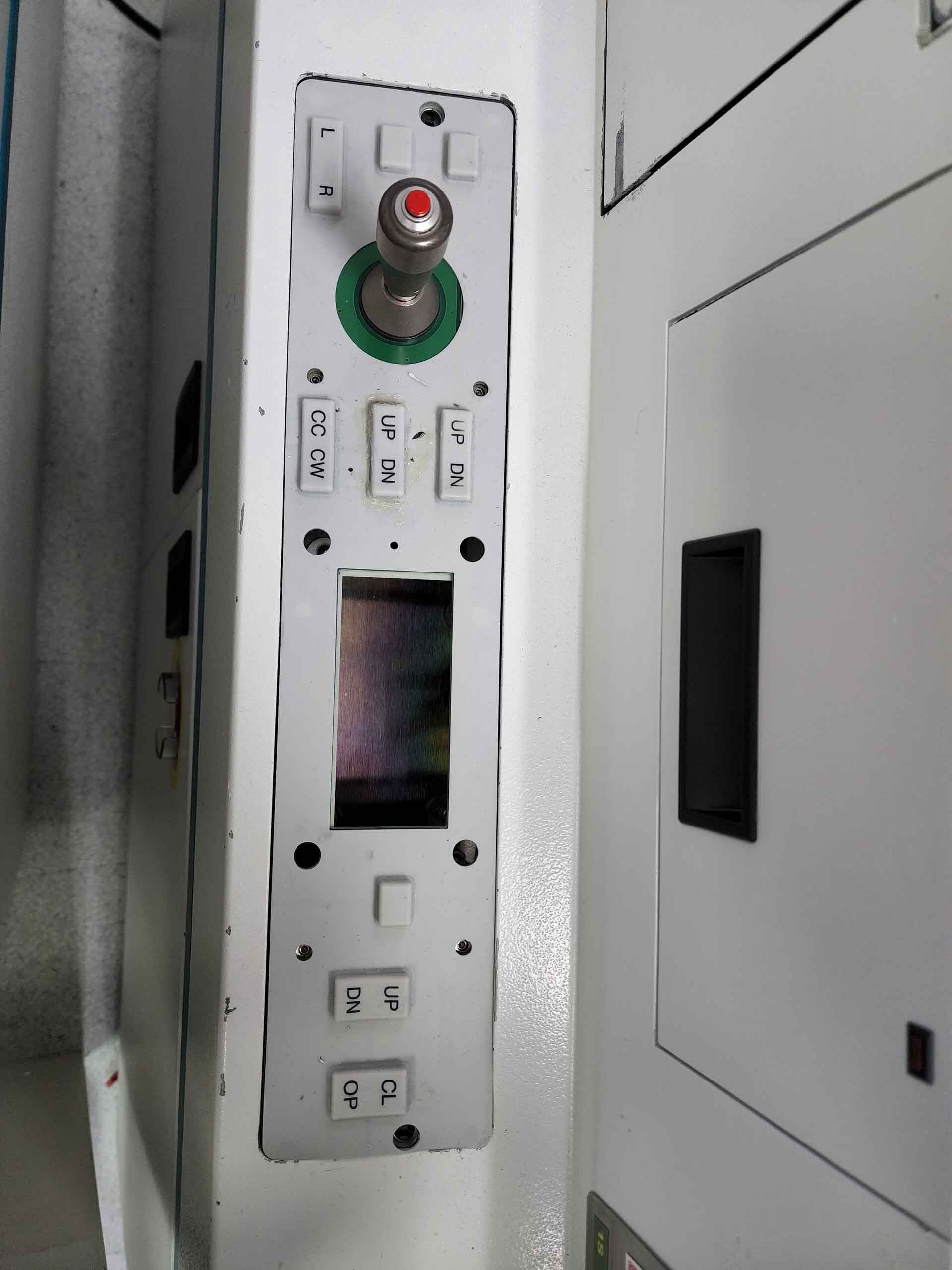
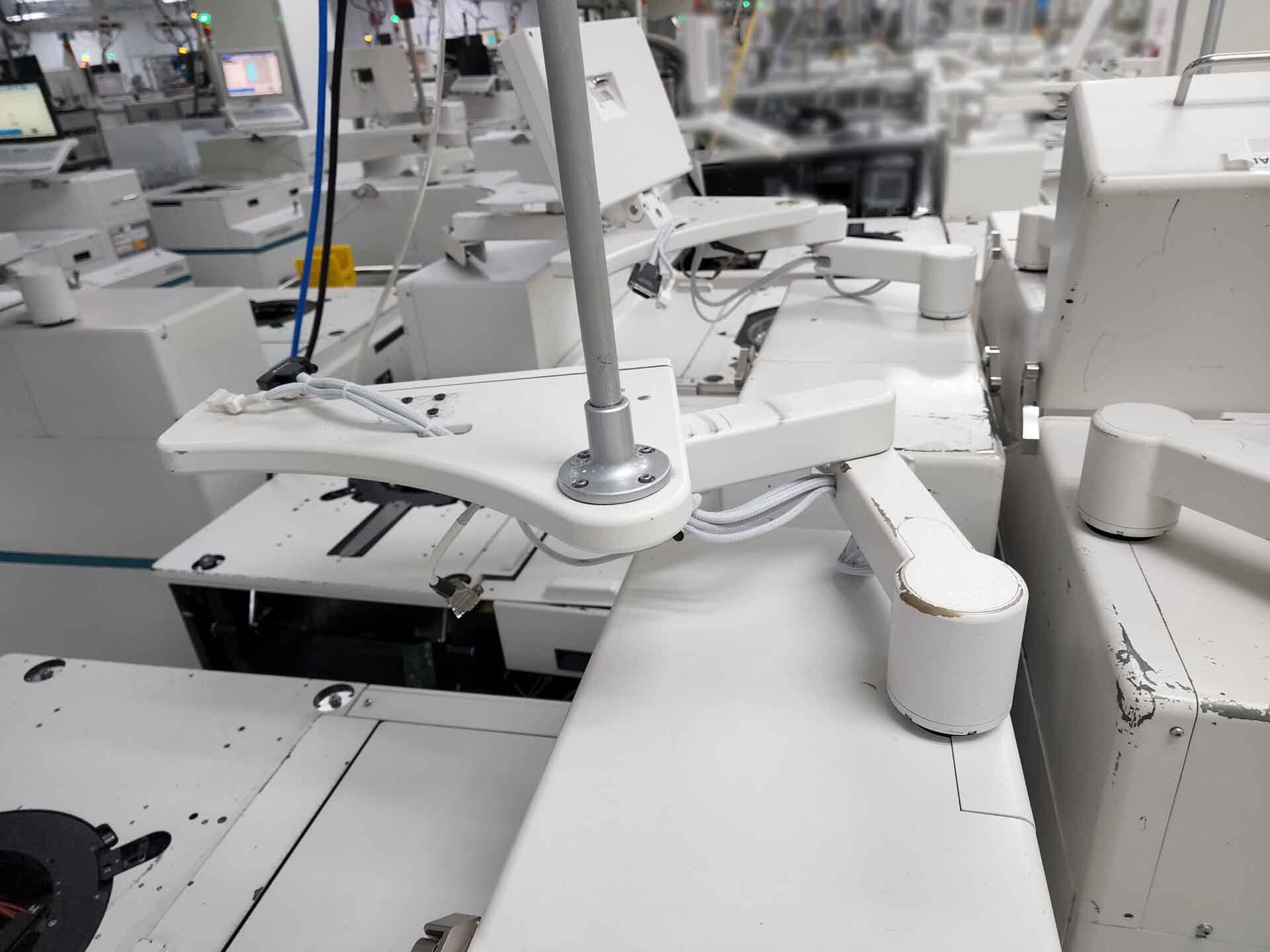
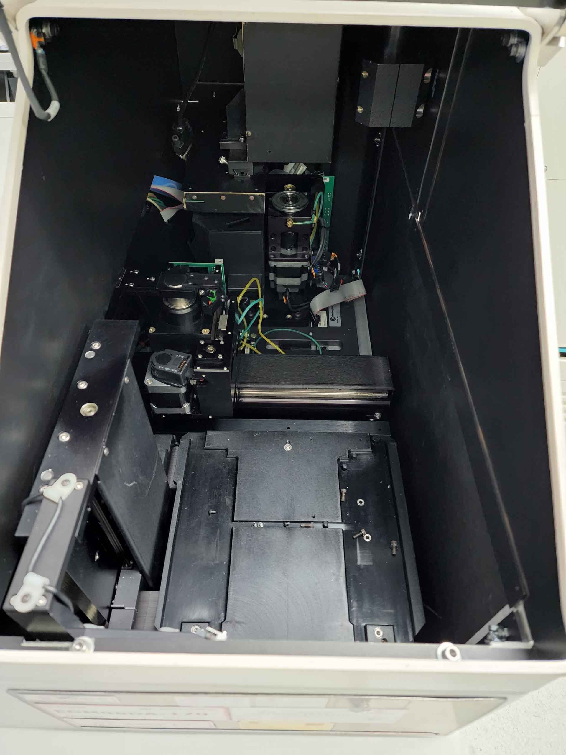
The Electro GlasELECTROGLAS / EG 4090u prober is an industry-leading, automated solution for semiconductor wafer probing and testing. It is designed for high-precision process control and data analysis, providing flexible and cost-effective automation of wafer testing procedures. Featuring a state-of-the-art robotic staging equipment, refined wafer handling and testing protocols, advanced automatic alignment algorithms and integrated data acquisition systems, EG 4090u prober delivers unprecedented accuracy and performance. ELECTROGLAS 4090 U prober employs a true, full 5-axis motion control system, allowing for multi-axis movement of both stage and chuck. This allows for precise, automated alignment of samples and contact tips, as well as precise scanning, scrubbing and probing operations. The unit also offers an integrated, 1 degree-of-freedom center guiding mechanism for precise wafer handling and positioning. The prober also features an advanced, in-built data acquisition machine and optional integrated data display, data logger, software management and communication functions. The data acquisition tool features a fast sample clock able to meet the most demanding throughput requirements. With the proprietary GView software, users can accurately re-construct part geometry, trace paths during testing and verify test performance. Integrated with 4090u prober is a powerful, automated SCARKerchie Optimal Probing Asset, providing optimal model-based electrical testing of wafers and devices. By combining the advanced motion control model and axial probing, it allows for reliable and accurate testing even in challenging environments and with complex sample geometries. 4090 U has a configurable wafer handling plate and offers flexible calibration and auto-scanning functionality for both 2D and 3D applications. As well, it allows for reliable, easy-to-perform manual alignment, with a high-precision beam-splitter X-Y alignment camera used for optimal results. With the cost-effective, powerful and highly efficient ELECTROGLAS / EG 4090 U prober, semiconductor testing is easily automated and reliable. Digital image analysis, statistical analysis algorithms and powerful data analysis tools provide unmatched accuracy and process control.
There are no reviews yet
