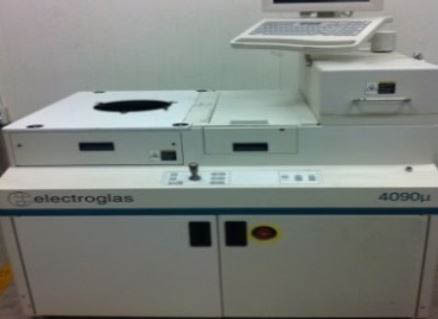
Used ELECTROGLAS / EG 4090u #9074280 for sale
URL successfully copied!
Tap to zoom


ID: 9074280
Wafer Size: 8"
Auto probe station, 8"
TEMPTRONIC Tri-temp gold chuck top assy
Cassette loader
GPIB / RS232C / TTL Tester interface
Temperature range: - 40°C to +150ºC
PZ-7 Z-Stage
Z Resolution: 0.125 Mil
PTPA (Probe To Pad Alignment), PTPO
Display control module with EG Commander 7.3 for DOS
Vision module with dual bridge CCD Camera assy
LCD Touch screen monitor
OCR
Air dryer
TEMPTRONIC TPO3000A Chiller
Input voltage: 220 VAC, 50/60 Hz, Single phase.
ELECTROGLAS / EG 4090u is a prober designed for the testing and probing of both single- or multi-site devices on wafer substrates. It uses proprietary electrical characterization technology to provide comprehensive, repeatable characterization which can be applied across a wide range of materials. EG 4090u is built on a modular platform, allowing for ease of installation and reconfiguration. It supports a wide range of high frequency probing solutions that can be tailored to any board or device. High voltage probing is available, with sustained high voltage rates up to 500V DC. Multi-site probing is enabled through the use of a switch matrix and up to 256 probe sites. The fingertip and linear probes provide superior resolution and repeatability, delivering quick probing times and high accuracy. The design of ELECTROGLAS 4090 U includes advanced robotic positioning and self-aligning equipment, which improves reliability and repeatability of probing. ELECTROGLAS 4090u has an embedded control system that allows for control and data collection from multiple wafer substrates. This unit is highly configurable and offers a range of performance-enhancing options that help ensure a high return on investment. The Electrical Measurement (EM) module is included with the installation of EG 4090 U. This provides an interface between the prober control machine and electrical measurement tools for electrical characterization. It supports a wide range of electrical hardware and software, allowing for both automated measurements and manual control. 4090 U also comes with automated wafer handling, with up to 8 wafers in a contiguous pattern and automated loading and unloading of wafers. This allows for repeatable and rapid probing across multiple wafer substrates. In addition, ELECTROGLAS / EG 4090 U features advanced wafer mapping that allows for quick and accurate mapping of multiple sites on a single wafer. This is especially beneficial for yield optimization and process failure analysis. Overall, 4090u is an advanced and reliable prober that is well suited for detailed probing and electrical characterization of both single- and multi-site devices on wafer substrates. Its advanced features and automated wafer handling can help accelerate the rate of throughput and yield optimization.
There are no reviews yet