Used ELECTROGLAS / EG 4090u #9210101 for sale
URL successfully copied!
Tap to zoom










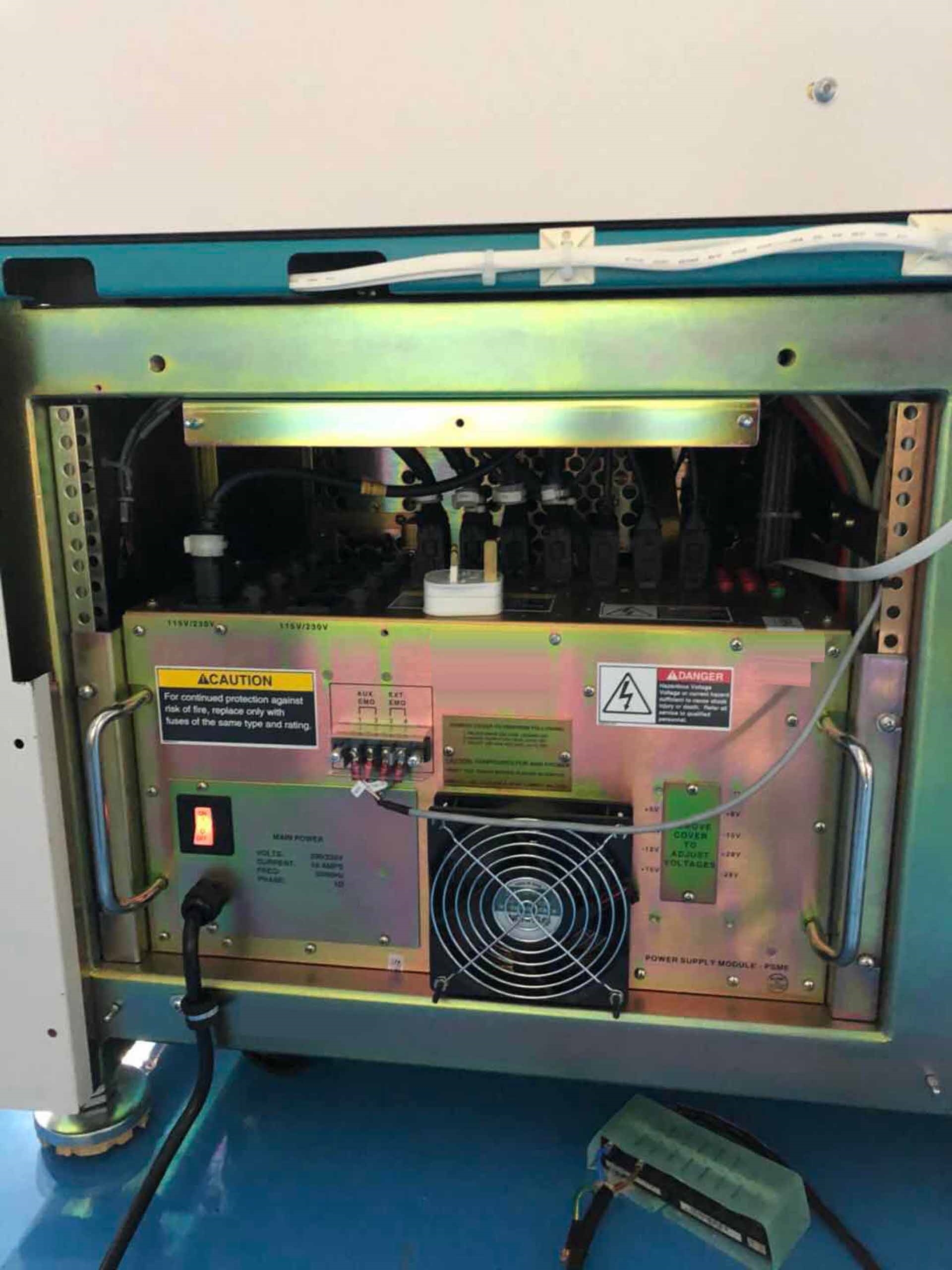

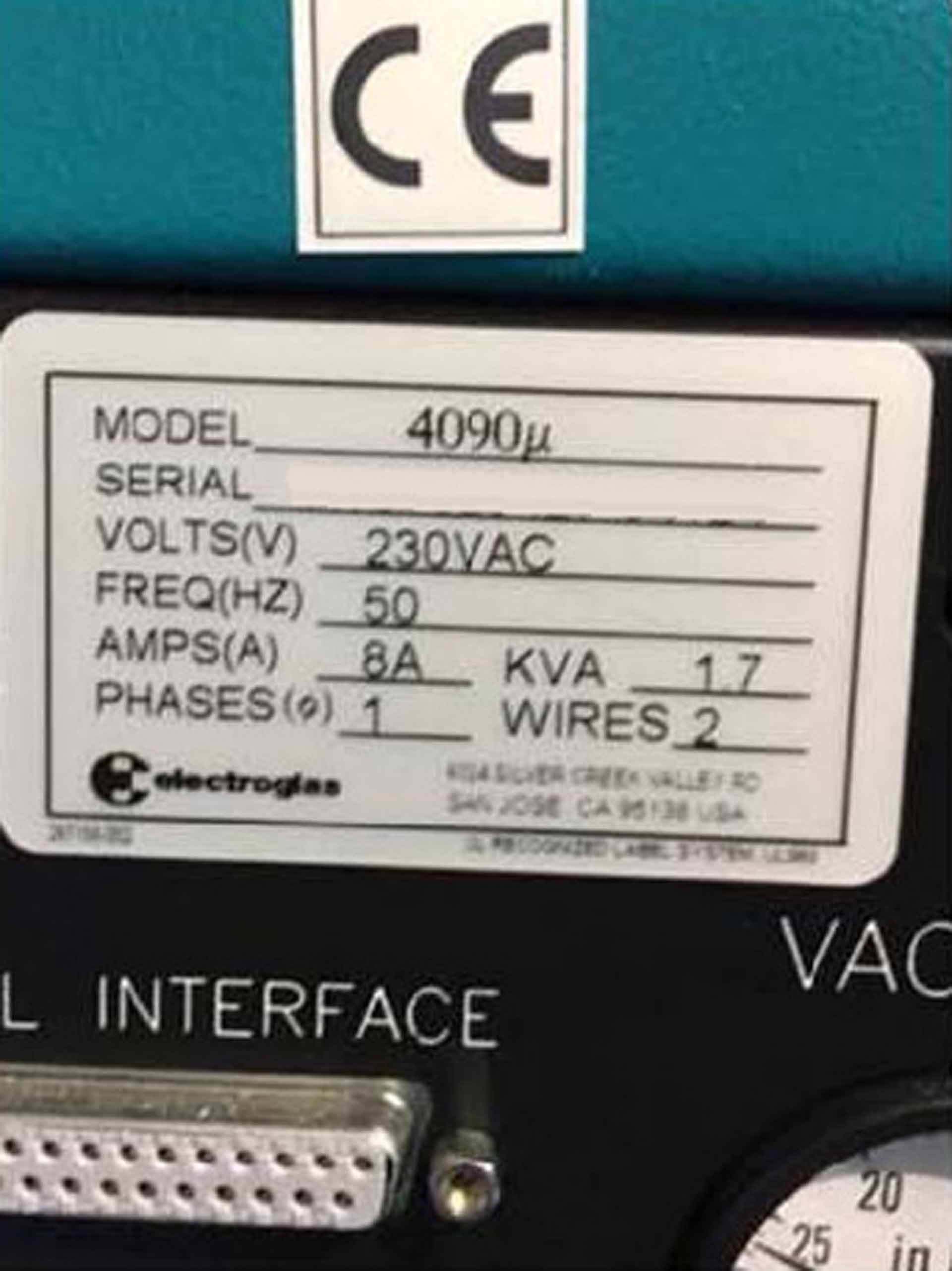

ID: 9210101
Wafer Size: 4"-8"
Probers, 4"-8"
Cassette: 25 or 26 Slots
Sequential
Programmable access controllable via external I/O
Auxiliary wafer tray
Quick single wafer insertion and extraction
Cross slot wafer detection
Intelligent quick load pipelining
Closed loop material handling
Accuracy: ±4 μm (System accuracy includes X, Y, ø / Z)
XY Positioning:
Travel: 19.80” (503 mm) X, 9.42” (239 mm) Y
Maximum speed: 10.0 in/sec (254.0 mm/sec)
Resolution: 0.01 mils (0.25 μm)
Repeatability: 0.01 mils (0.25 μm)
Maximum acceleration:
Standard configuration: 1.1G X axis, 0.53G Y axis
High force configuration: 0.88G X axis, 0.42G Y axis
Z-Stage:
Resolution Z: 0.25 mil 0.125 mil
Load:
Std. Z-stage: 25 lbs (11.3 kgs) 40 lbs (18.0 kgs)
HFZ-2: 135 lbs (61 kgs) 154 lbs (70 kgs)
Speed: 390 μsec/step 390 μsec/step
Probing range: 200 mil (5.1 mm) 200 mil (5.1 mm)
Travel full: 400 mil (10.2 mm) 400 mil (10.2 mm)
Repeatability Z: 0.25 mil (6.4 μm) 0.125 mil (3.2 μm)
ø Travel: ±5° ±5°
ø Resolution: 0.000917°/step 0.000917°/step
Chuck tops:
Standard: Ambient probing
Hot: Ambient to 130°C
Specials: Other ranges (Hot and cold)
Low compliance chuck tops: With HFZ-2 only
Standard: Ambient probing
Hot: Ambient to 130°C
Available in Au, Ni, Al (Unplated)
Tester communications:
Tester interfaces / Protocols supported
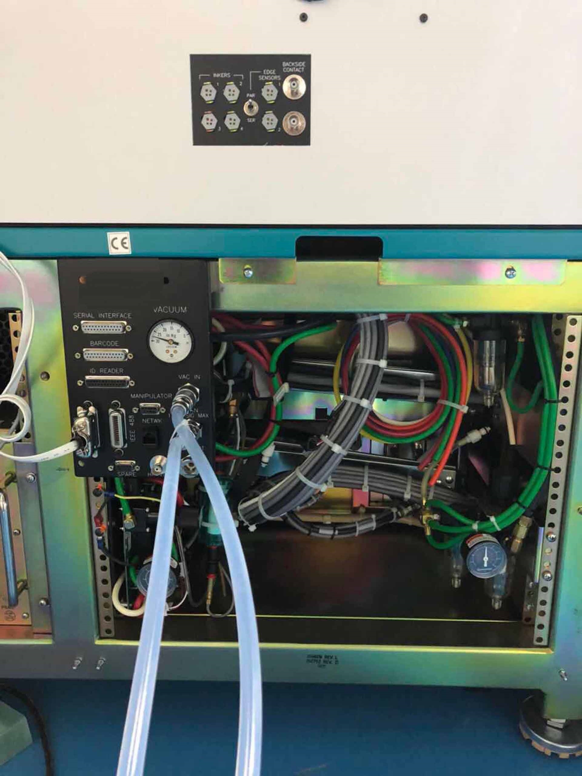
RS232C
TTL (Parallel I/0)
GPIB (IEEE-488)
EG Enhanced
RDP
Automation:
PTPA: Probe to pad alignment
Aluminized wafer
DPS II: Direct probe sensor II
APPV: Automatic probe position verification
PTPO: Probe to pad optimization
OCR: Optical character recognition
PMI: Probe mark inspection
IDI: Ink dot inspection
STAA: Self teach auto align
WSSC: Wafer stepping and scaling calibration
APCC: Automatic probe cleaning and continuity pad
CPCS II: Chuck probe contact sensor II
BSBC: Back side bar code reader
System architecture:
Multiple processors base around Pentium core
Flash memory (Core program)
PCI Bus internal PCBs (Serial and video)
PCI Bus ethernet PCB providing 10 and 100 MHz I/O speeds
Interface capabilities:
Tester interface packages
Motorized probe card theta
Semi automatic probe card
GEM: Generic equipment model
SEMI Standard communications for factory automation and control
AUI: Advanced user interface
FPD: Flat panel display, 10.4” Active matrix display
Touch screen
Elastomer keyboard
Clean room compatible
AT Style
Tester communications:
Tester interfaces and protocols supported
RS232C, TTL (Parallel I/0), GPIB (IEEE-488)
EGEnhanced, RDP
Prober mini-environment (Class 1):
Up to class: 10,000 areas
Electrical:
Volts Amps Hz
100 16.5 50/60
115 15.0 50/60
230 7.5 50/60
Footprint:
Standard: 45.3” (115 cm) W x 35.2” (89.4 cm) D x 34.2” (88 cm) H
Mini-e/SMIF: 52.5” (133.4 cm) W x 35.2” (89.4 cm) D x 34.2 (88 cm) H
Air: Minimum 85 psi CDA, 1.0 SCFM
Vacuum: Minimum 22 in Hg, 1.25 SCFM (Momentary flow for 15 sec).
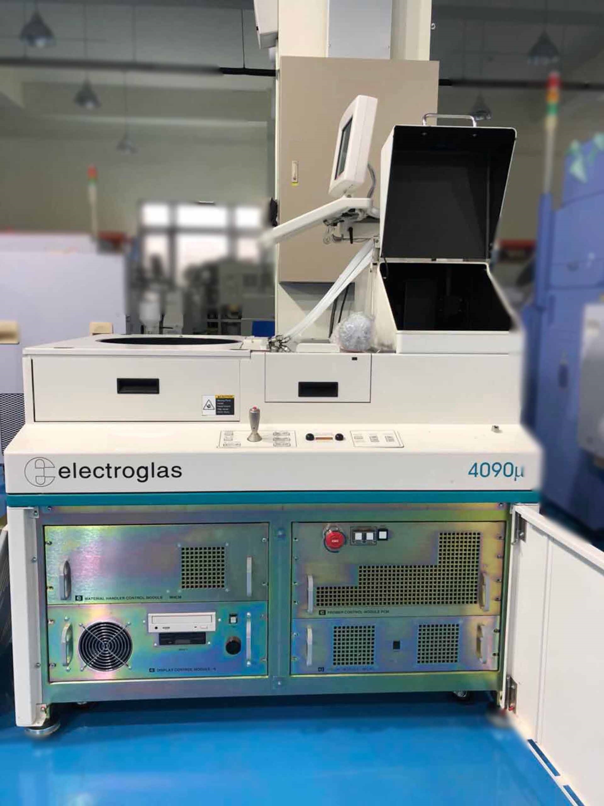
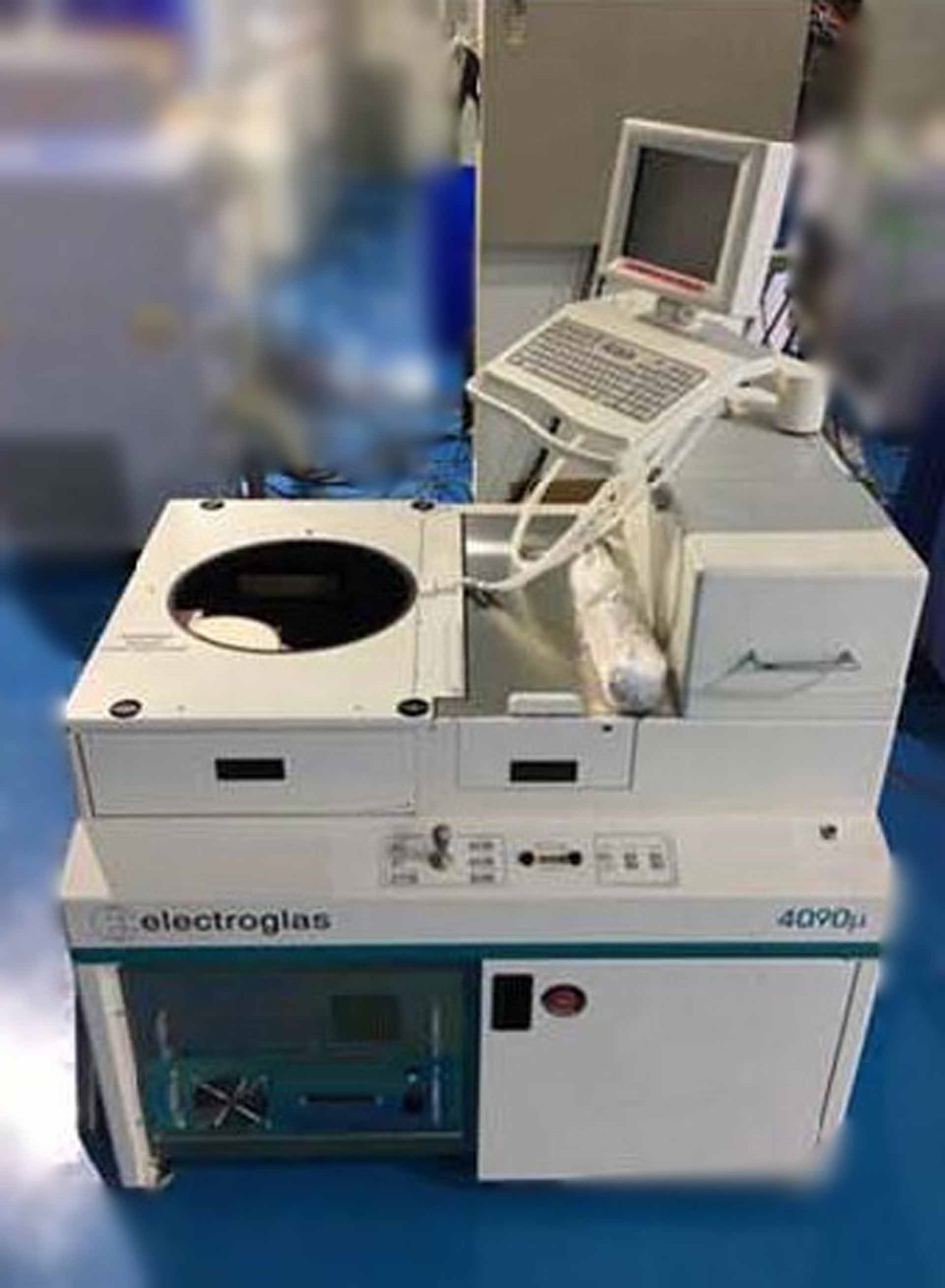
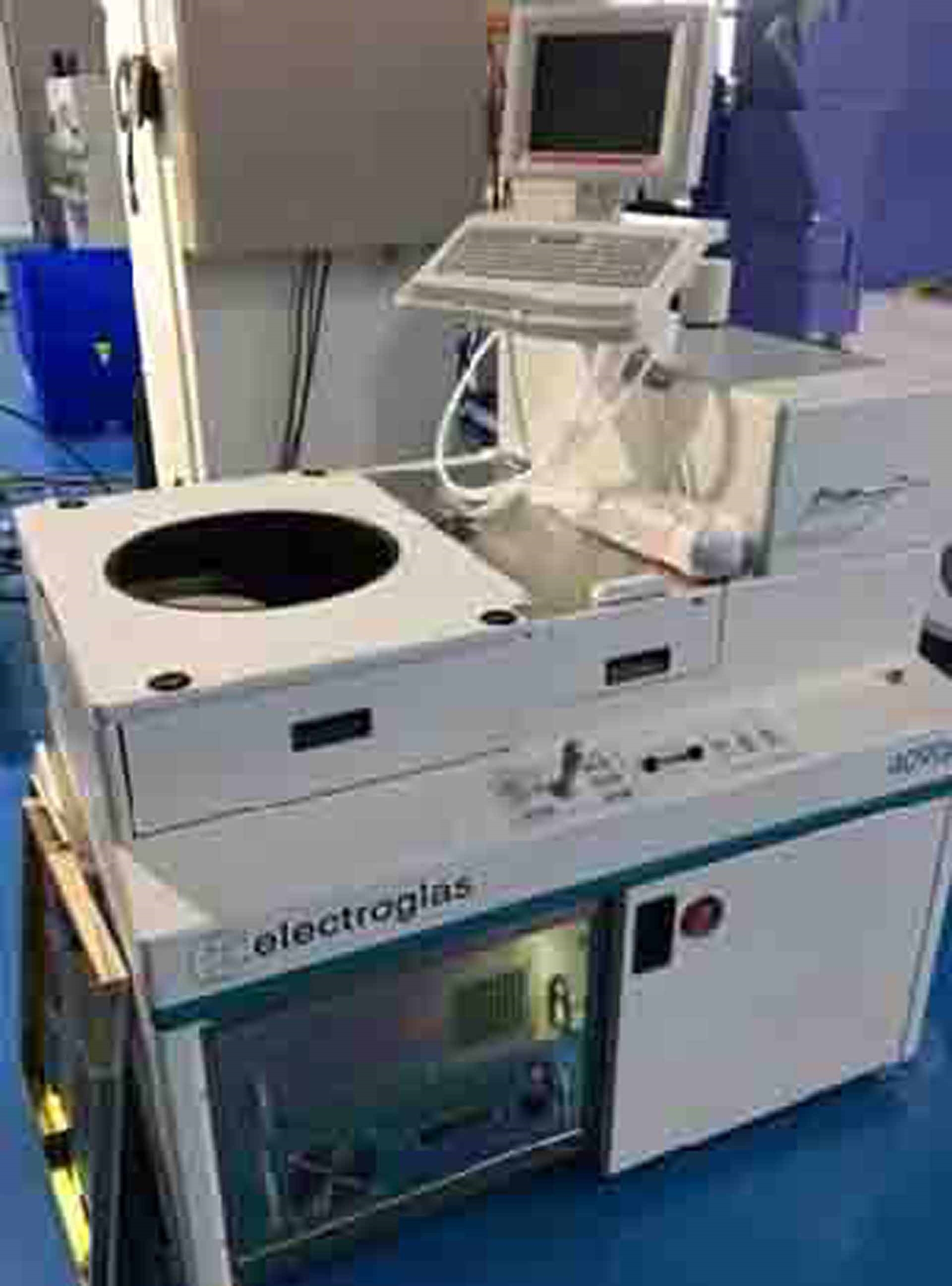
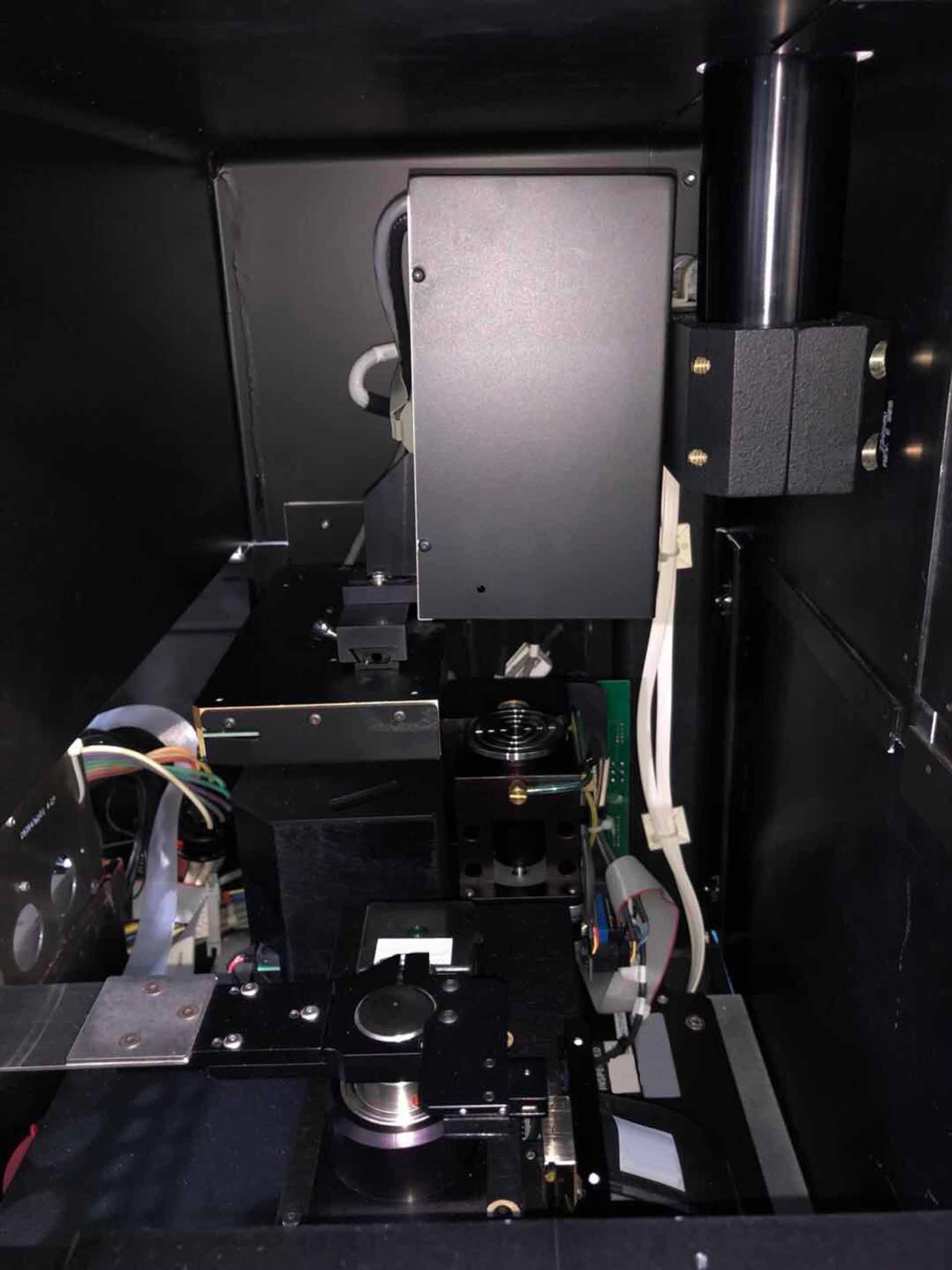
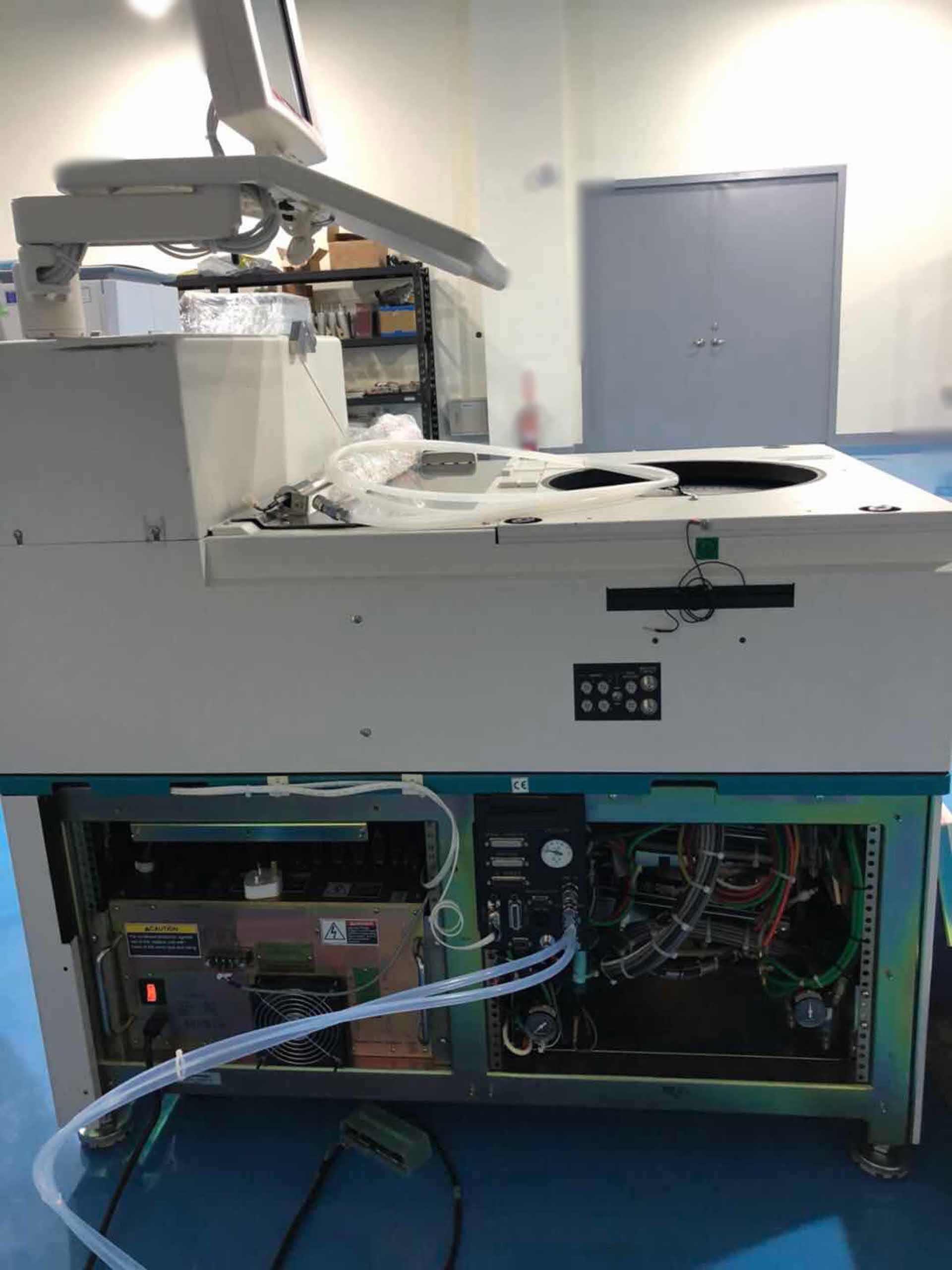
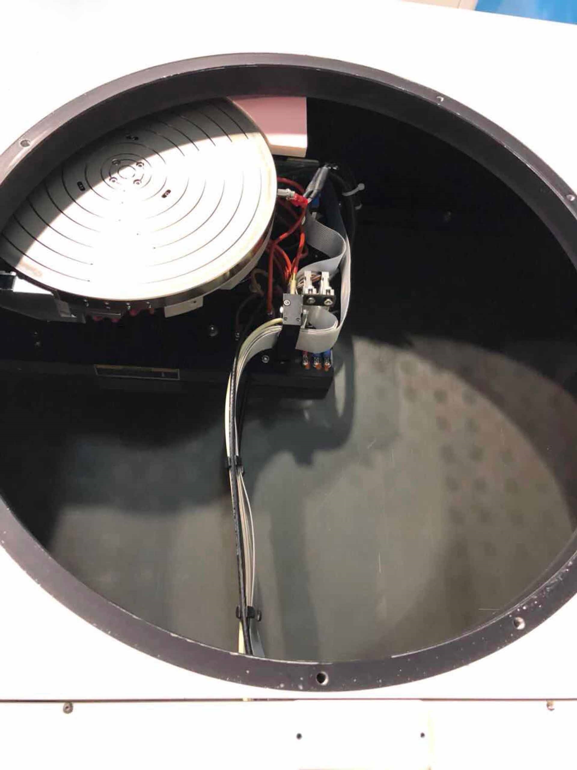
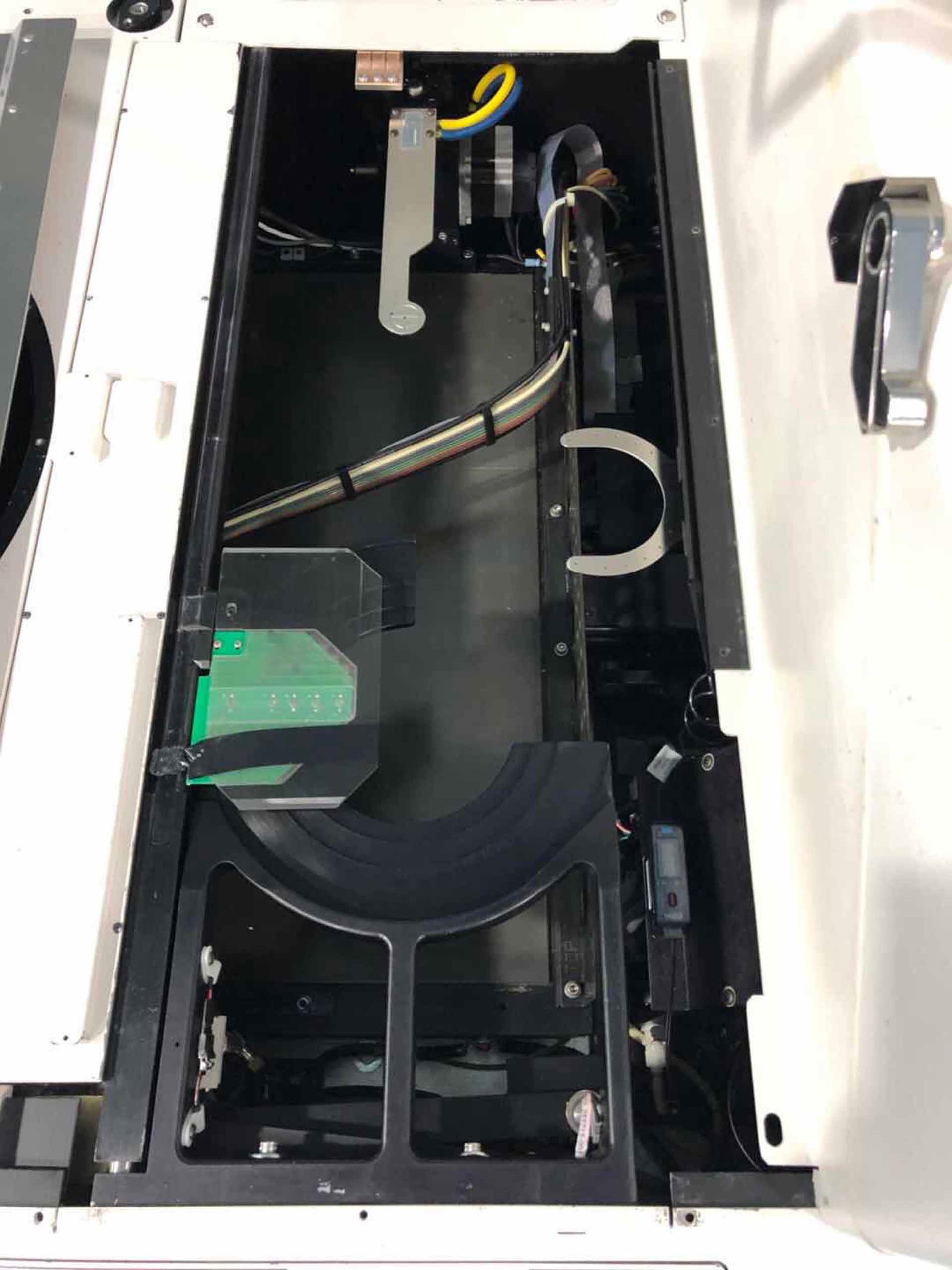
ELECTROGLAS / EG 4090u prober is a comprehensive system designed for automated testing of semiconductor wafers and devices. This advanced system provides both optical and electrical probing capabilities, allowing for the precise characterization of a broad range of devices. EG 4090u is equipped with multiple heads, allowing access to multiple probes and rapid results. It comes equipped with a number of application-specific features, including a high-resolution differential input bridge, advanced electronic scanning capabilities, and an integrated high-accuracy temperature controller. ELECTROGLAS 4090 U's high-resolution differential input bridge provides digital-to-analog conversion and linear amplification. This feature helps deliver extremely accurate and repeatable results, allowing precise control over the measurement range and voltage. 4090u's bridge also features programmable thresholds for indicating events and setting minimum/maximum values. ELECTROGLAS / EG 4090 U offers powerful electronic scanning capabilities that enable powerful characterization capabilities on a wide range of semiconductor devices. The scanning functions feature a wide range of functions, including oscilloscope-style measurement of time, frequency, and switching characteristics. This feature can also be configured to measure capacitance, inductance, and low-level current signals. In addition to its powerful electronic scanning features, ELECTROGLAS 4090u comes equipped with an integrated high-accuracy temperature controller. This controller ensures that the temperature is maintained at a consistent level during testing. This feature allows for faster device characterization and testing cycles. 4090 U is an advanced prober system that is well-suited for testing and characterizing a broad range of semiconductor devices. Its combination of optical and electrical probing capabilities, as well as its electronic scanning and temperature control features, make it an ideal tool for accurate and repeatable testing.
There are no reviews yet


