Used KARL SUSS / MICROTEC PA 200 #293742056 for sale
URL successfully copied!
Tap to zoom
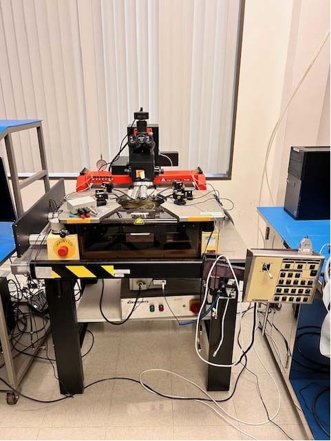

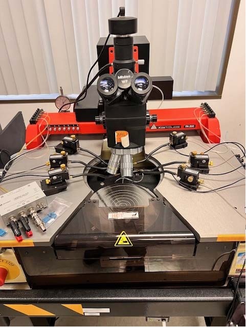
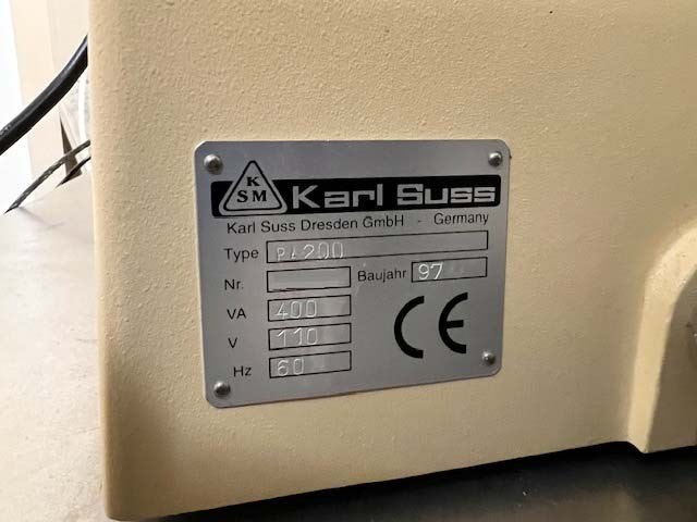
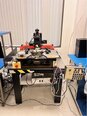
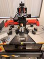
KARL SUSS / MICROTEC PA 200 is a prober that is used in the fabrication process of high-end semiconductor components. It plays an integral part in bringing designs to life, as it permits the probing of semiconductor wafers in a precise and reliable manner. This equipment also enables operators to conduct a variety of tests in order to assess the quality of the semiconductors produced on the fabrication line. The prober utilizes a complex, multi-axis robot system to move the workpiece, typically a semiconductor wafers, from the input hopper to the probe station.The robot is programmed to move the wafer to its designated target area where it is to be tested.This movement can be either manually or automatically by means of a manual joystick or by a computer controller system.Once the wafer is at the probing station, a plurality of probes, both manual and automated, can be used to characterized the wafer and measure its various electrical parameters. MICROTEC PA 200 has numerous advanced features designed for maximum reliability, accuracy and speed. For instance, it offers a DC/RF signal generator capabilities, which can be used to drive input signal into a device under test.It also houses a mechanical scanner, with a trigger signal to synchronize scanning and data transfer. The scanner is made of solid titanium alloy and is equipped with a feedback system for measuring mechanical deflection and resolution.Moreover, it comes with a graphical user interface (GUI) for an easy setup, advanced probing options and data manipulation capabilities. KARL SUSS PA-200 is a highly reliable and precise prober that is capable of handling advanced probing applications. It is particularly beneficial in the production of extremely high-end components, ensuring a high level of accuracy and safety during the production process. This prober offers semiconductor manufacturers an exceptional balance between high speed, reliability, low maintenance and precision, making it a reliable, yet cost-effective tool for probing semiconductor wafers in the fabrication process.
There are no reviews yet