Used SEMICS OPUS3-SD(e) #293828463 for sale
URL successfully copied!



Tap to zoom
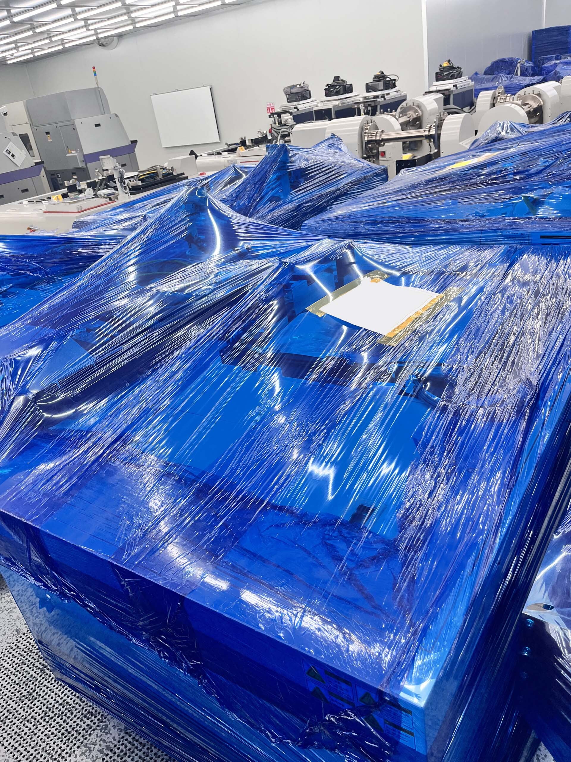

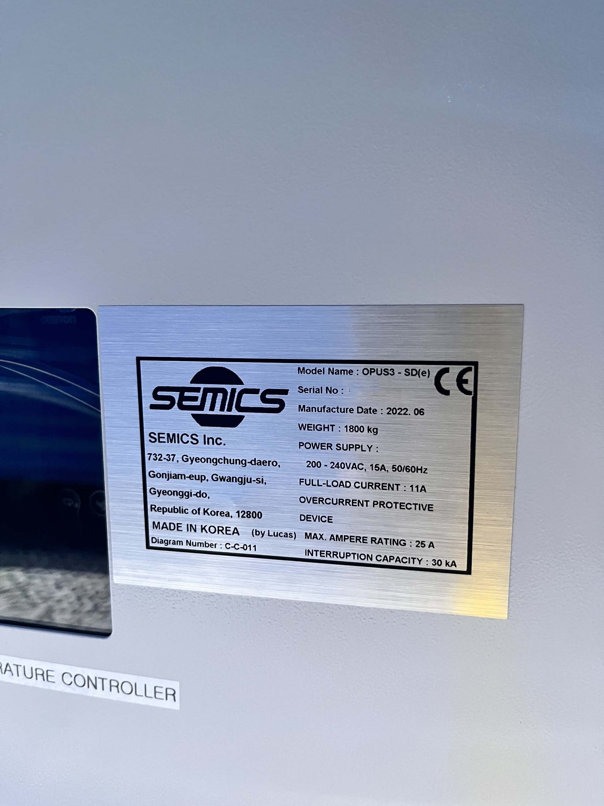
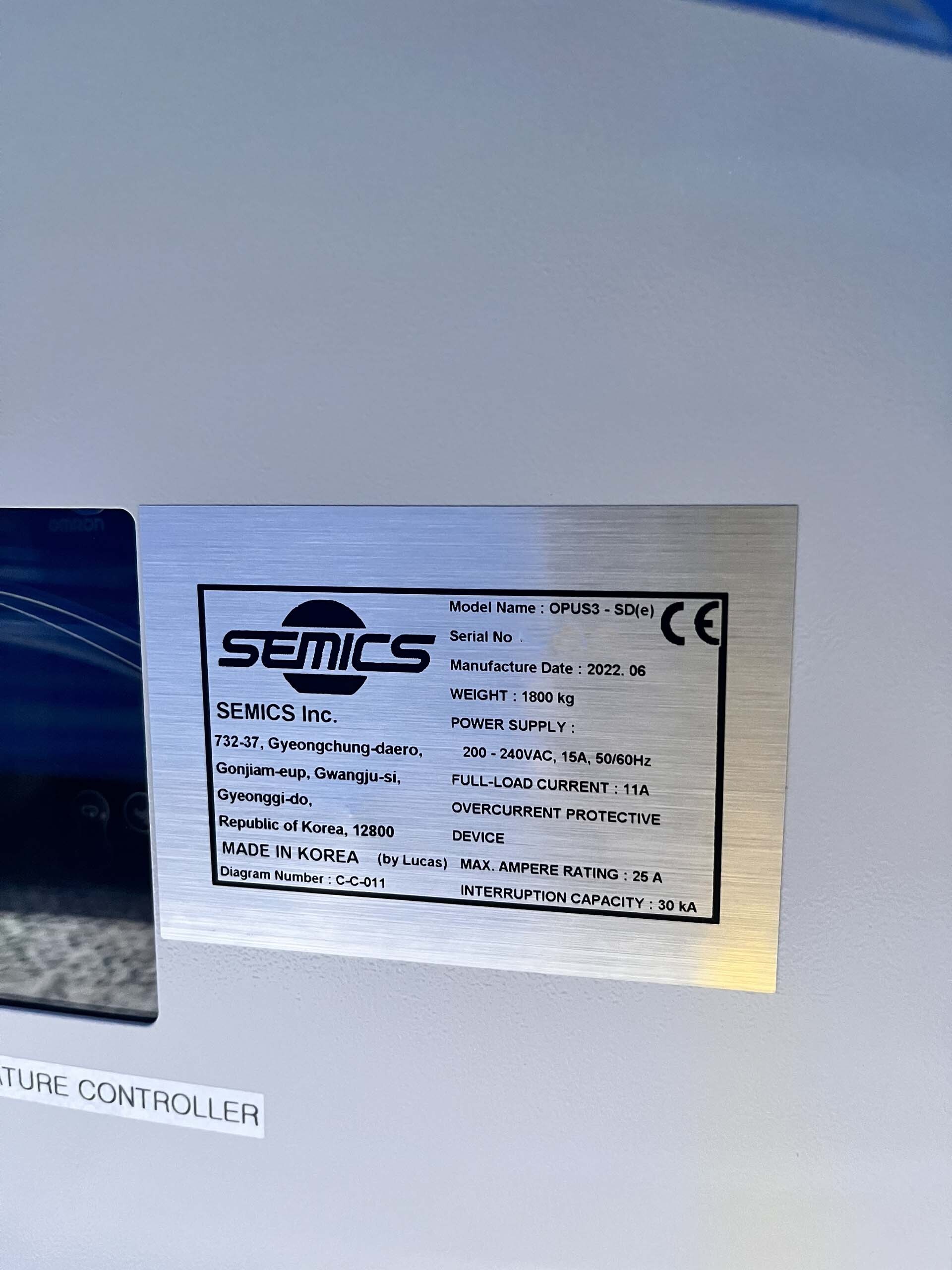
SEMICS OPUS3-SD(e) is a high-performance prober designed for semiconductor testing applications, offering advanced capabilities for precise and efficient wafer probing processes. This prober is developed by SEMICS, a leading provider of semiconductor test equipment, known for its innovative solutions in the field of semiconductor testing. The OPUS3-SD(e) prober is designed to facilitate the testing of semiconductor wafers, ensuring accurate measurement and analysis of electrical characteristics of semiconductor devices on the wafer. The prober is equipped with advanced features and functionalities to support various testing requirements in semiconductor manufacturing and research environments. One of the key features of SEMICS OPUS3-SD(e) prober is its high-precision probing capability, which allows for accurate and reliable contact with individual devices on the wafer. The prober is equipped with advanced positioning systems and alignment mechanisms to ensure precise contact with the test points on the wafer, minimizing the risk of measurement errors and ensuring consistent and reliable test results. The OPUS3-SD(e) prober also offers a high level of automation and programmability, allowing users to customize and automate the probing process according to their specific testing requirements. The prober can be easily integrated with test systems and software platforms, enabling seamless communication and data exchange between the prober and other testing equipment in the semiconductor testing environment. In addition to its precision and automation capabilities, SEMICS OPUS3-SD(e) prober is also known for its high-speed probing capability, allowing for rapid testing of multiple devices on a wafer. The prober is equipped with advanced probing mechanisms and control systems to ensure fast and efficient probing processes, reducing test time and increasing overall throughput in semiconductor testing operations. Furthermore, the OPUS3-SD(e) prober is designed to handle a wide range of wafer sizes and types, making it a versatile solution for semiconductor testing applications. The prober is equipped with interchangeable chuck systems and wafer handling mechanisms to support different wafer sizes and materials, providing flexibility and scalability for a variety of testing requirements. SEMICS OPUS3-SD(e) prober also incorporates advanced safety features and environmental controls to ensure reliable and safe operation in semiconductor testing environments. The prober is designed to meet industry standards for safety and performance, with built-in protections and monitoring systems to prevent damage to the wafer and the prober during testing. Overall, SEMICS OPUS3-SD(e) prober is a state-of-the-art solution for semiconductor testing, offering advanced capabilities for precise, efficient, and reliable wafer probing processes. With its high-precision probing, automation, high-speed testing, versatility, and safety features, the OPUS3-SD(e) prober is a trusted tool for semiconductor manufacturers and researchers looking to achieve accurate and repeatable test results in their semiconductor testing operations.
There are no reviews yet