Used TAKAYA APT 8400 #293823261 for sale
URL successfully copied!
Tap to zoom
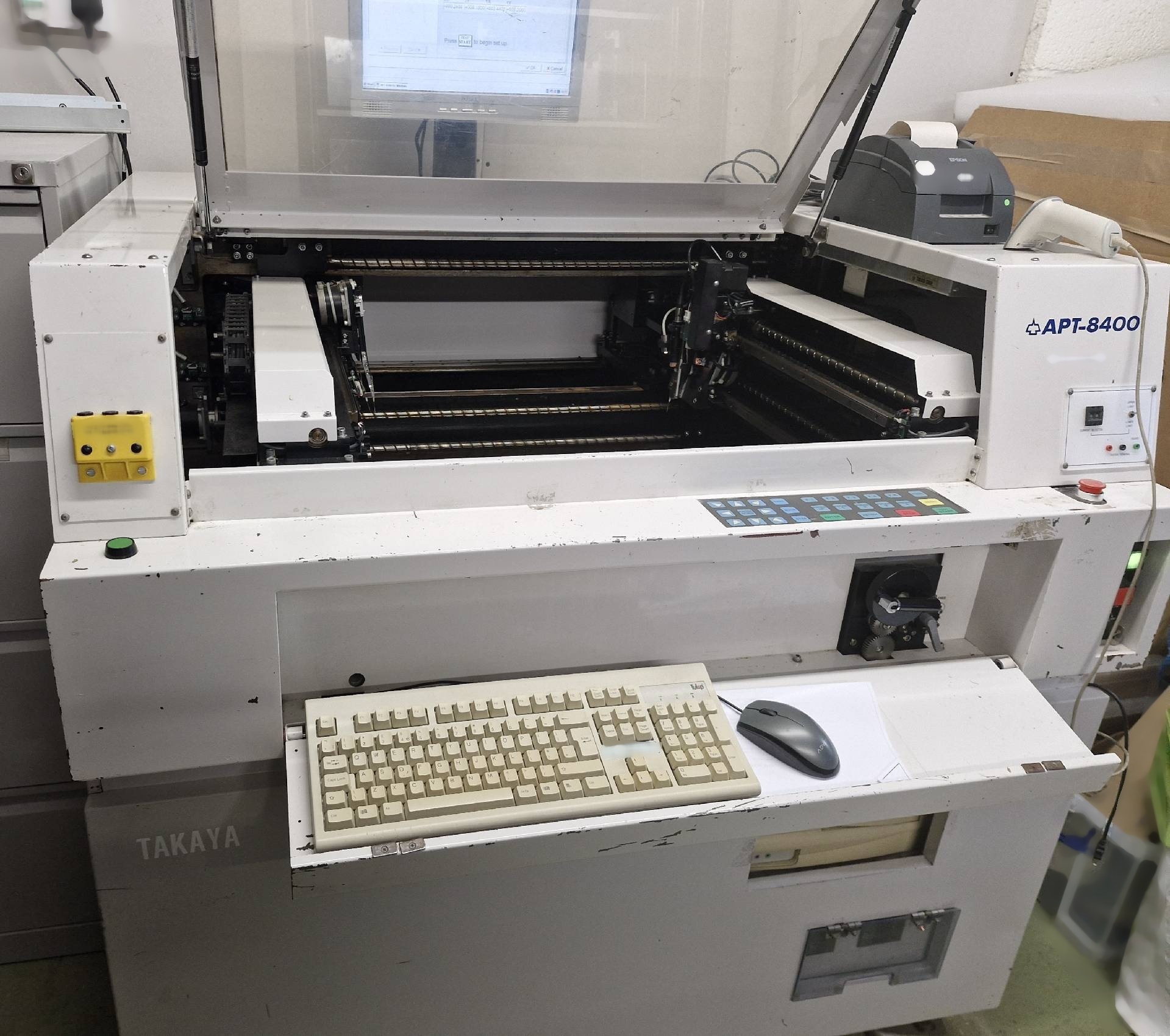

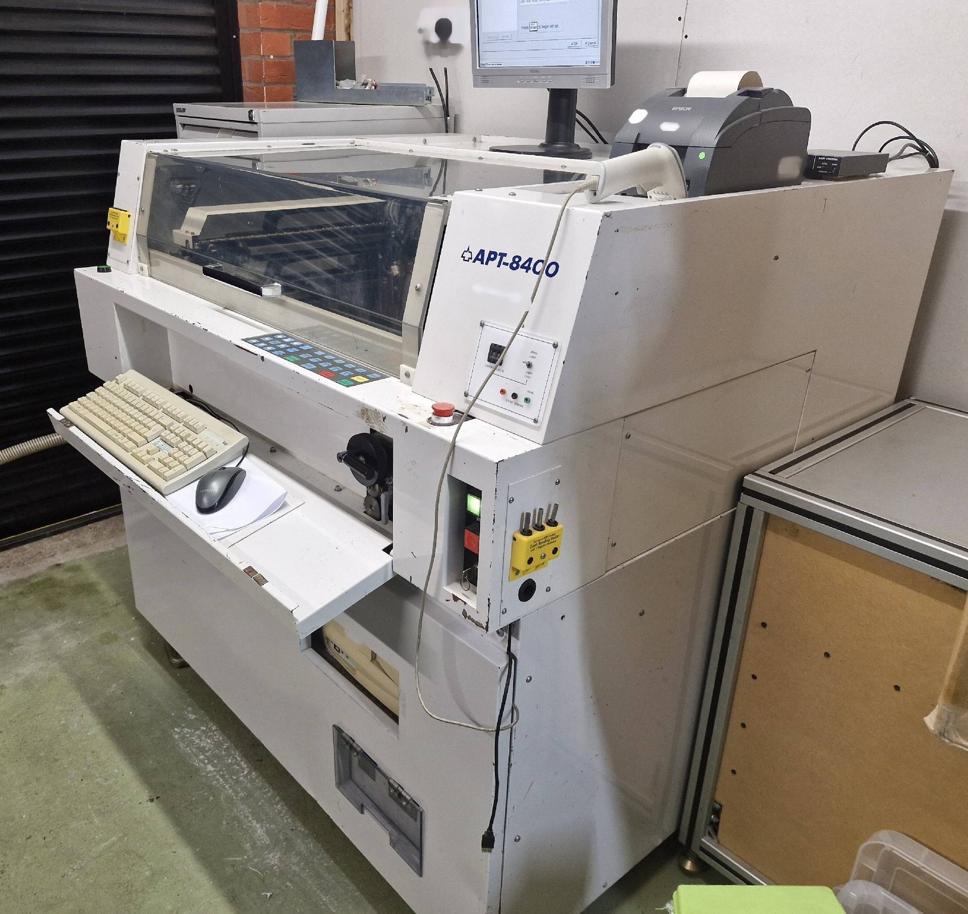
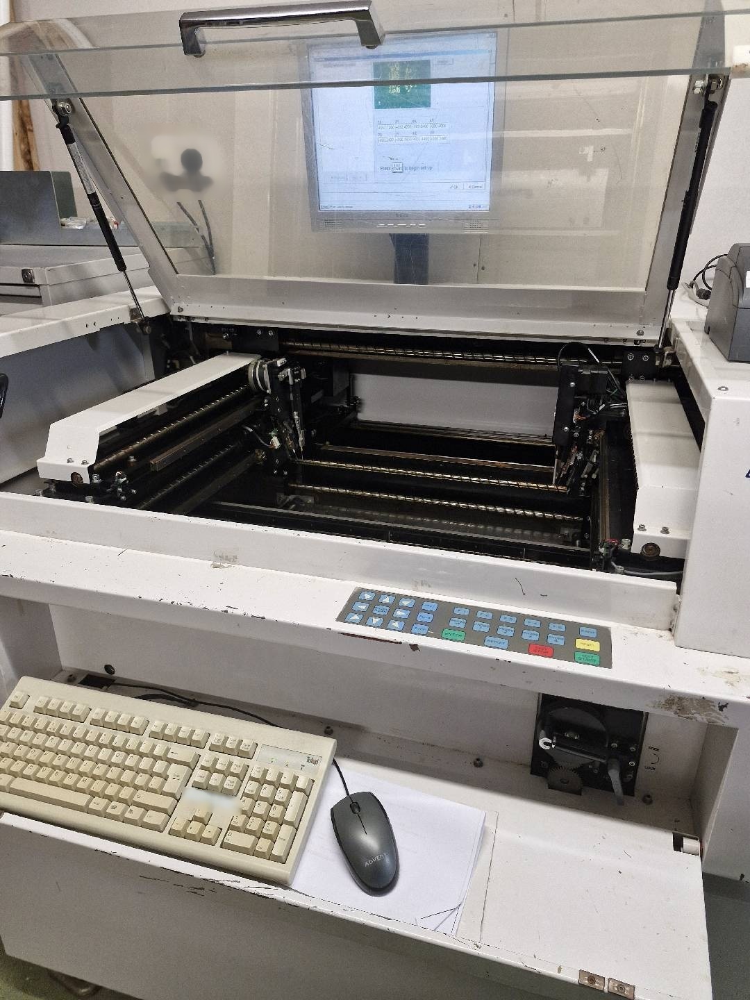
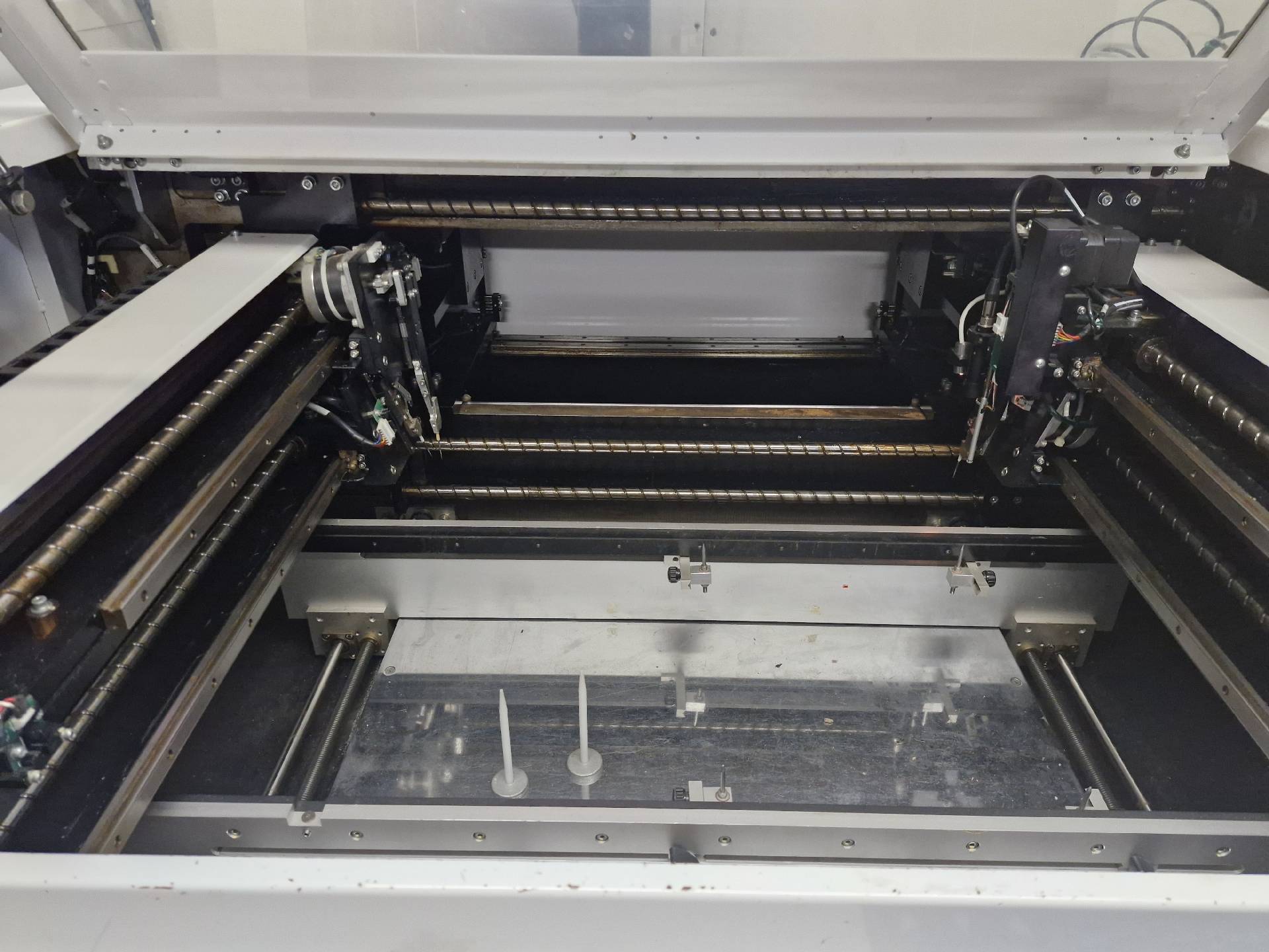
ID: 293823261
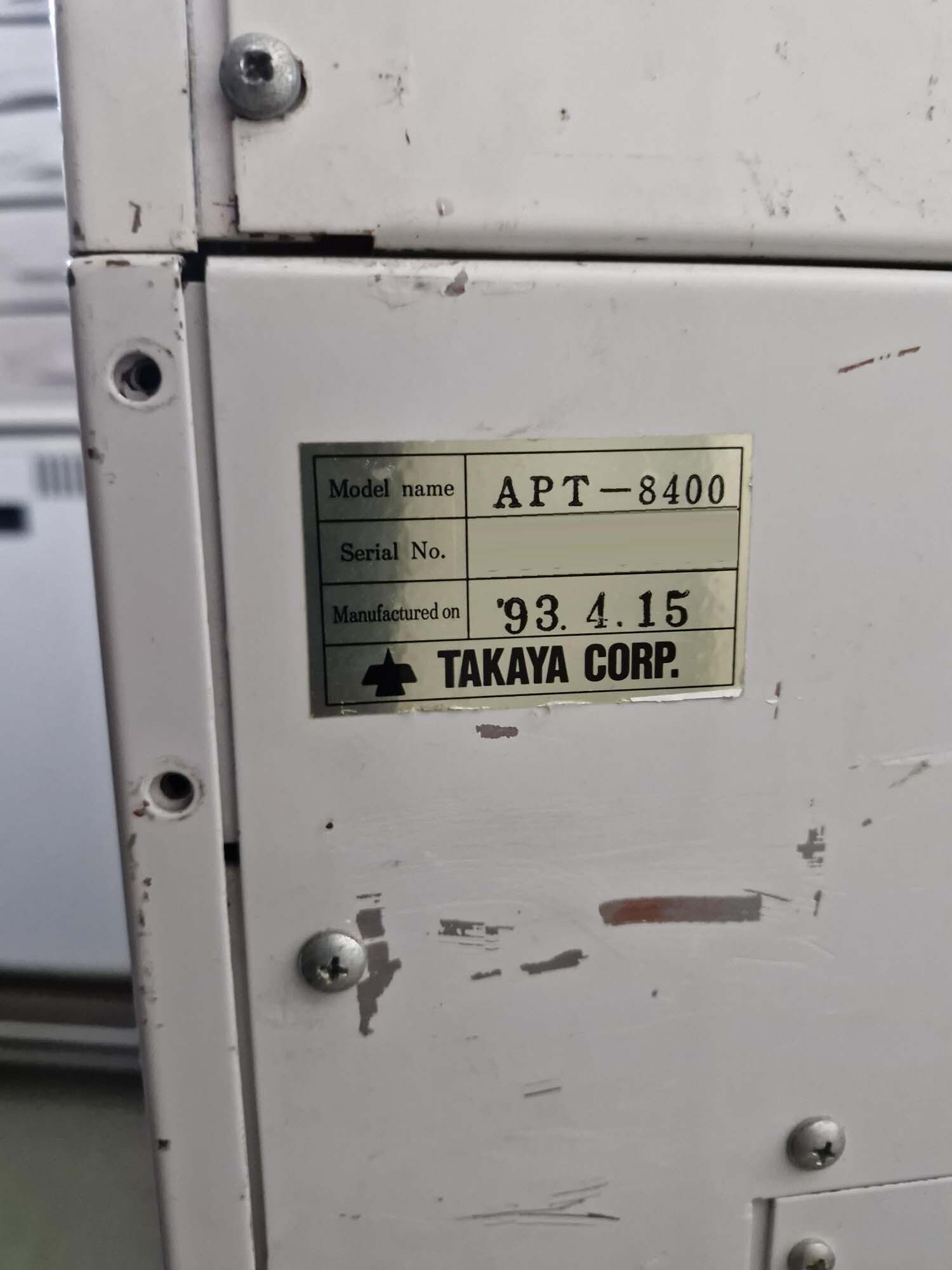
Vintage: 1993
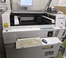
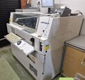
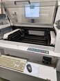
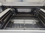
Flying prober
(4) Moving contact probes
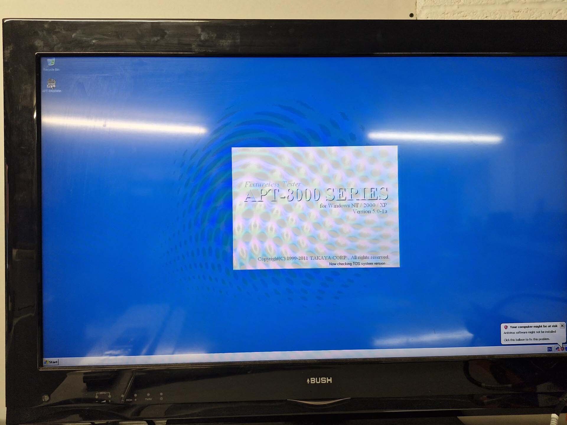
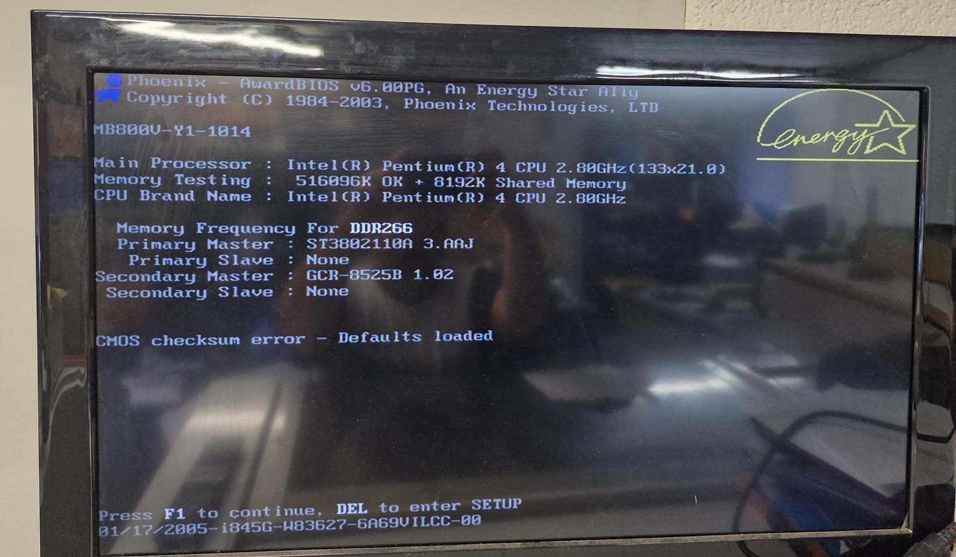
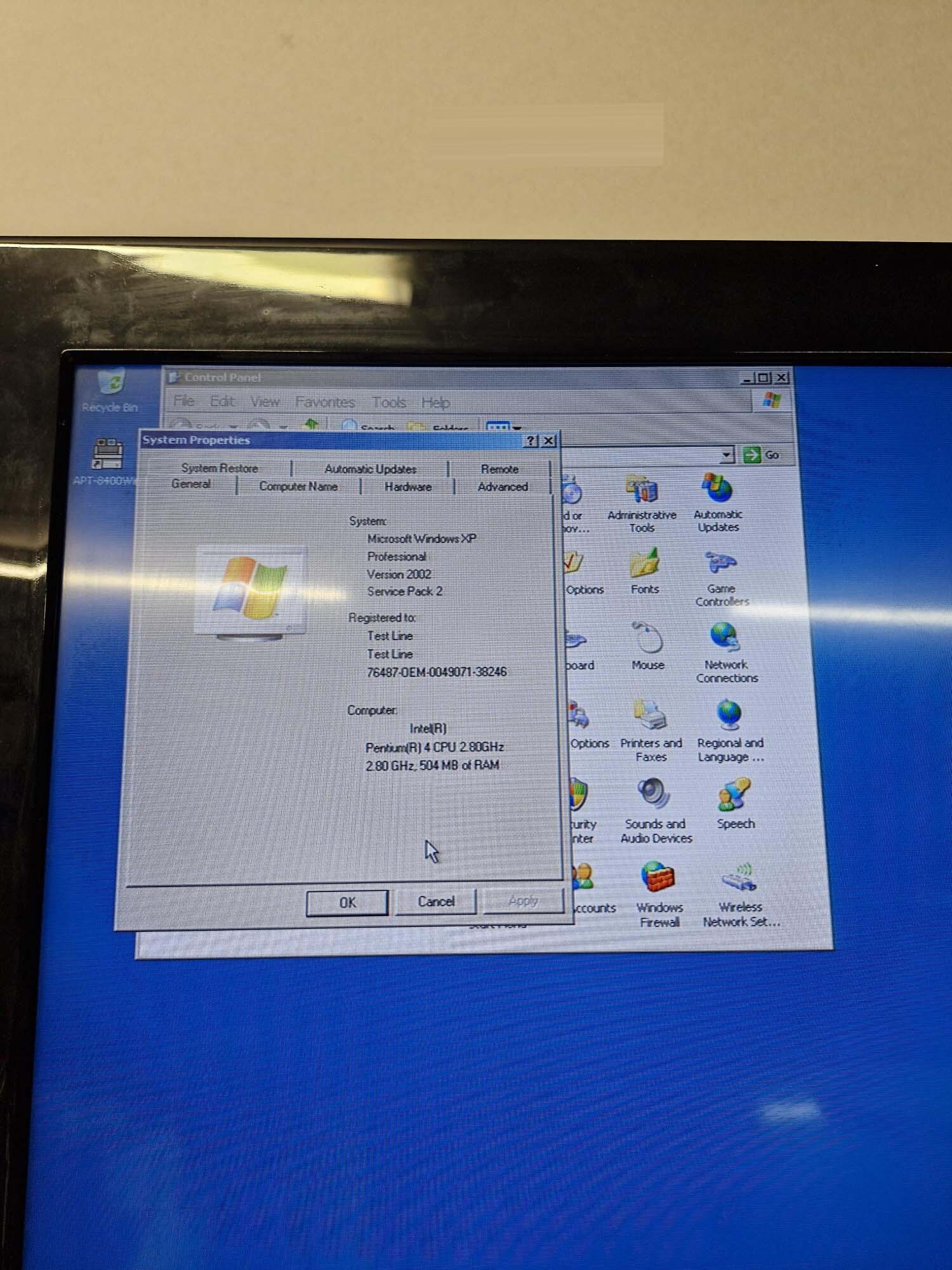
PC
Keyboard
1993 vintage.
TAKAYA APT 8400 is a prober designed for unconventional high-precision probing, inspection and testing of microelectronics and semiconductor devices. It offers flexibility and high accuracy with its superior multi-zone high resolution design and prolonged focus arm. Featuring a 5-zone advanced imaging system, APT 8400 can accurately measure thin-film photomasks and wafers, with resolutions to 0.5 micron. Its unique multi-zone architecture allows optimal recovery of signal and minimizes the impact of off-axis signals which results in diverse and critical source and measure operations. Its extended probing ranges provides an increased comfort rating to the user and increased dimensional measurement accuracy. The 8400 features an integrated two-axis rotary stage that makes it suitable for 3D measurements. The axis rotates upon contact with the part, providing precise positioning of the probe tip. It has built-in alignment and image analysis functions, allowing for accurate inspection of multiple parts with the same geometry. TAKAYA APT 8400 prober is capable of fast signal testing and analysis applications, allowing for maximum production throughput. It supports signal analysis with fast data acquisition systems and a spectral analyzer, for signal amplitude and purity monitoring. It also offers flexible multiple parameter setting options for optimal measurement results. The prober is designed for ease of use with an intuitive graphical user interface and ergonomic navigation. It supports several automated task capabilities such as programmability, automation script functions and parameter setting. Additionally, the 8400 is equipped with variability-tolerant positioning and micro-alignment technology, ensuring accurate measurement and testing of difficult geometries. Overall, APT 8400 is a powerful and precise prober that is suitable for inspection and testing of complex geometries of microelectronics and semiconductor devices. Its multi-zone imaging system, extendable probing range and intuitive GUI makes it a powerful choice for improved process control, accuracy and repeatability.
There are no reviews yet