Used TEL / TOKYO ELECTRON P-12 #293771412 for sale
URL successfully copied!
Tap to zoom
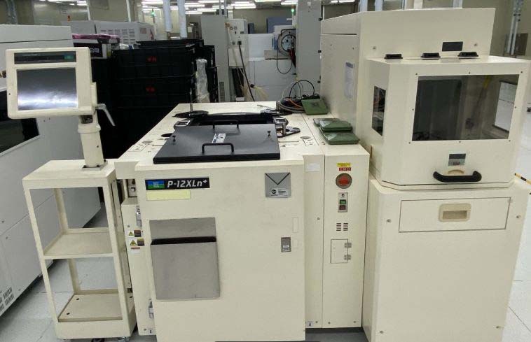

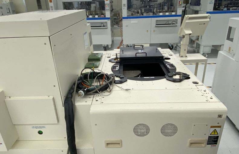
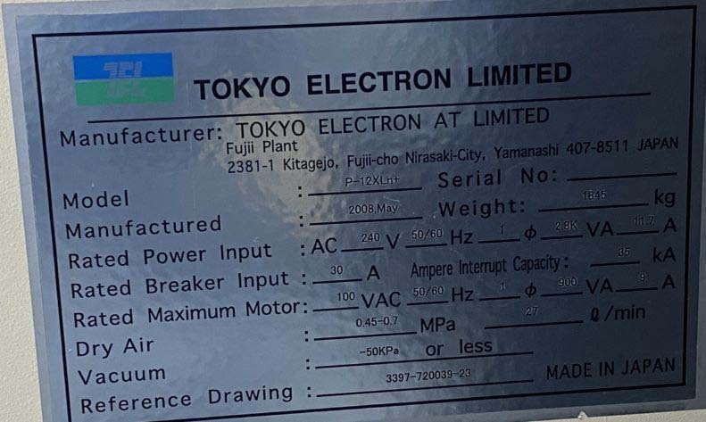
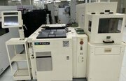
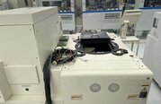
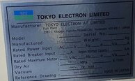
TEL / TOKYO ELECTRON P-12 is an advanced prober system designed for semiconductor testing and inspection applications. This prober combines precision engineering, advanced automation, and innovative technology to ensure high-performance and accuracy in wafer testing processes. TEL P-12 is equipped with a range of features and capabilities that make it a versatile and reliable tool for semiconductor manufacturing companies. TOKYO ELECTRON P-12 prober system is designed to handle a variety of wafer sizes, from small to large wafers, with high precision and repeatability. It features a robust and stable wafer chuck mechanism that allows for secure wafer handling and positioning during testing. This ensures that the prober can accurately probe each die on the wafer without any misalignment or errors. One of the key features of P-12 prober is its advanced probing capability, which allows for high-speed and high-accuracy testing of semiconductor devices. The prober is equipped with a sophisticated probing mechanism that can quickly and accurately make contact with each die on the wafer, enabling fast and efficient testing processes. This high-speed probing capability is essential for ensuring fast throughput and high productivity in semiconductor manufacturing facilities. In addition to its probing capabilities, TEL / TOKYO ELECTRON P-12 prober also offers advanced automation features that streamline the testing process and reduce the need for manual intervention. The prober is equipped with robotic arms and advanced software algorithms that can automatically load and unload wafers, position the probe tips, and perform testing sequences without operator intervention. This automation capability helps to increase efficiency, reduce human error, and improve overall testing throughput. TEL P-12 prober is also designed to be flexible and adaptable to a range of different testing requirements. It offers a variety of probing configurations, including single-site probing, multi-site probing, and dynamic probing, which can be customized to suit the specific needs of different semiconductor devices and applications. This flexibility allows semiconductor manufacturers to optimize their testing processes and achieve higher yields and reliability in their products. Furthermore, TOKYO ELECTRON P-12 prober is equipped with advanced software tools and diagnostics capabilities that enable real-time monitoring and control of the testing process. The prober can collect and analyze data during testing, identify potential issues or defects, and provide feedback to operators for immediate action. This real-time monitoring capability helps to ensure that any problems are quickly addressed, minimizing downtime and maximizing testing efficiency. Overall, P-12 prober is a state-of-the-art testing tool that offers high precision, accuracy, and throughput for semiconductor manufacturing companies. Its advanced probing capabilities, automation features, flexibility, and real-time monitoring capabilities make it an invaluable asset for wafer testing processes, helping companies to achieve higher yields, faster time-to-market, and superior product quality in today's competitive semiconductor industry.
There are no reviews yet