Used TEL / TOKYO ELECTRON P-12 #293771821 for sale
URL successfully copied!
Tap to zoom
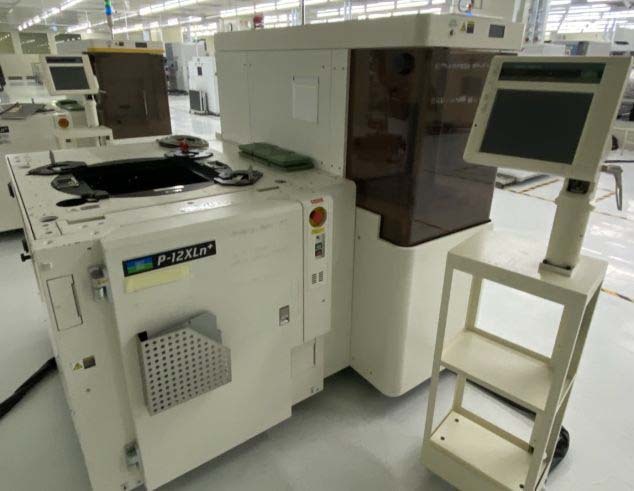

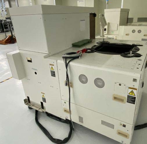
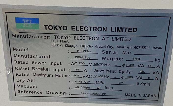
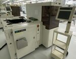
TEL / TOKYO ELECTRON P-12: A Comprehensive Analysis of a Prober TEL P-12 is a state-of-the-art prober designed for semiconductor testing and evaluation. This advanced equipment is utilized in the semiconductor industry for probing wafers to identify and troubleshoot any faults or defects in the integrated circuits (ICs) before final packaging. Key Features: TOKYO ELECTRON P-12 is equipped with a range of innovative features to ensure accurate and efficient probing of wafers. One of its key features is the high-precision positioning system, which allows for precise alignment of the probe needles with the pads on the wafer. This ensures that each probe makes contact with the desired test point, enabling accurate measurements to be taken. The prober also features a high-speed probing capability, allowing for rapid testing of wafers without sacrificing accuracy. This is essential in the semiconductor industry, where time-to-market is a critical factor in ensuring competitiveness. Another key feature of P-12 is its modular design, which allows for easy customization and expansion. This enables semiconductor manufacturers to tailor the prober to their specific requirements, ensuring optimal performance and efficiency in their testing processes. Furthermore, the prober is equipped with advanced software that provides users with real-time monitoring and control capabilities. This allows operators to quickly identify and address any issues that may arise during the probing process, minimizing downtime and maximizing productivity. Applications: TEL / TOKYO ELECTRON P-12 is used in a wide range of semiconductor testing applications, including wafer-level testing, device characterization, and failure analysis. Its high-precision probing capabilities make it ideal for probing small and densely-packed ICs, ensuring accurate and reliable test results. The prober is commonly used in the production of various semiconductor devices, including memory chips, processors, and sensors. Its ability to quickly and accurately test these devices is essential for ensuring their quality and reliability before they are integrated into end products. Overall, TEL P-12 plays a crucial role in the semiconductor industry, enabling manufacturers to test and evaluate their products with the highest level of precision and efficiency. Advantages: TOKYO ELECTRON P-12 offers several key advantages over traditional probing systems. Its high-precision positioning system and high-speed probing capability ensure accurate and efficient testing of wafers, reducing the risk of false positives or negatives in the test results. The prober's modular design and advanced software also provide users with a high degree of flexibility and control over the testing process. This enables semiconductor manufacturers to adapt the prober to their specific requirements, ensuring optimal performance and efficiency in their testing operations. Moreover, P-12 is designed for ease of use, with an intuitive user interface that simplifies the operation of the prober. This reduces the need for extensive training and allows operators to quickly become proficient in using the equipment. In conclusion, TEL / TOKYO ELECTRON P-12 is a cutting-edge prober that offers semiconductor manufacturers a range of advanced features and capabilities for efficient and reliable wafer testing. Its high-precision probing system, high-speed probing capability, and modular design make it an essential tool for ensuring the quality and reliability of semiconductor devices in the fast-paced and competitive semiconductor industry.
There are no reviews yet