Used TEL / TOKYO ELECTRON P-12 #293771822 for sale
URL successfully copied!
Tap to zoom
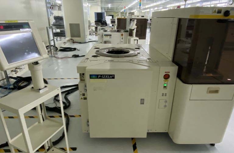

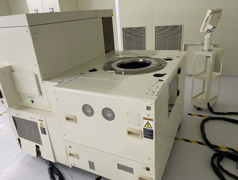
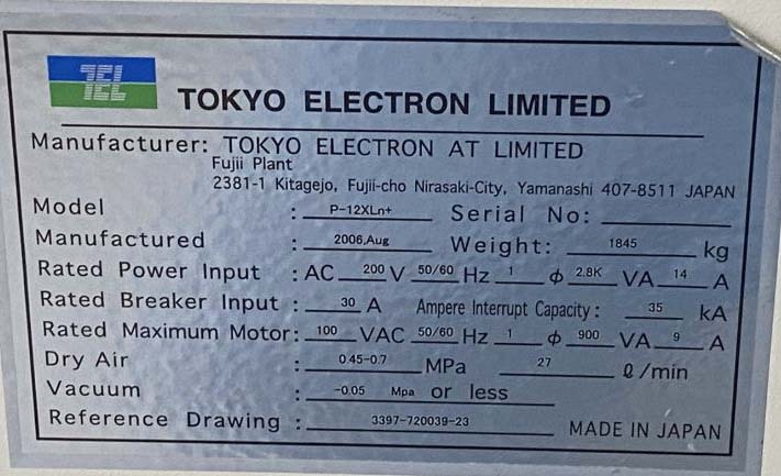
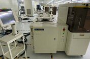
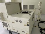
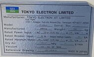
TEL / TOKYO ELECTRON P-12 is a highly advanced prober equipment that plays a crucial role in the semiconductor manufacturing process. The prober is an essential piece of equipment used to test and inspect semiconductor wafers before they are further processed into integrated circuits. This particular model, TEL P-12, is known for its unparalleled precision, reliability, and efficiency, making it a preferred choice for semiconductor manufacturers worldwide. One of the key features of TOKYO ELECTRON P-12 prober is its sophisticated design and precision engineering. This prober system is equipped with a high-precision robotic arm that can swiftly and accurately position the probe over the individual semiconductor dies on the wafer for testing. The advanced robotic arm is controlled by proprietary software algorithms that ensure precise alignment and contact with the test points on the wafer. In addition to its precise handling capabilities, P-12 prober also features a high-resolution vision unit that allows operators to visualize and inspect the semiconductor dies on the wafer before testing. This vision machine helps to identify any defects or irregularities on the wafer surface, enabling early detection and prevention of potential issues during the testing process. TEL / TOKYO ELECTRON P-12 prober is capable of handling wafers of various sizes, ranging from small to large diameters, making it a versatile solution for semiconductor manufacturers with diverse production needs. The prober can accommodate different wafer materials, including silicon, gallium arsenide, and other advanced semiconductor materials commonly used in the industry. One of the standout features of TEL P-12 prober is its advanced probing technologies, which enable high-speed and high-accuracy testing of semiconductor devices. The prober is equipped with multiple probe cards containing hundreds to thousands of micro-scale probes that make contact with the test points on the wafer. These probes are designed to deliver precise electrical signals for testing the functionality and performance of the semiconductor devices. TOKYO ELECTRON P-12 prober is also known for its superior performance in terms of throughput and efficiency. The prober tool is equipped with advanced automation features that streamline the testing process and minimize downtime. This results in higher productivity and faster time-to-market for semiconductor manufacturers, ultimately improving their competitiveness in the industry. Furthermore, P-12 prober incorporates advanced data acquisition and analysis capabilities, allowing real-time monitoring of test results and rapid feedback to optimize the testing parameters. The prober seamlessly integrates with software platforms for data management and analysis, enabling manufacturers to gather valuable insights into the performance and quality of their semiconductor devices. Overall, TEL / TOKYO ELECTRON P-12 prober is a state-of-the-art testing solution that offers exceptional precision, reliability, and efficiency for semiconductor manufacturers. With its advanced probing technologies, high-speed performance, and versatile handling capabilities, TEL P-12 prober is a valuable asset in the semiconductor manufacturing process, ensuring the production of high-quality and reliable semiconductor devices for various applications.
There are no reviews yet